ISL8011 データシートの表示(PDF) - Renesas Electronics
部品番号
コンポーネント説明
メーカー
ISL8011 Datasheet PDF : 10 Pages
| |||
ISL8011
Absolute Maximum Ratings (Reference to SGND)
Supply Voltage (PVIN, VCC) . . . . . . . . . . . . . . . . . . . . -0.3V to 6.5V
EN, MODE, PHASE, POR . . . . . . . . . . . . . . . . . . -0.3V to VCC+0.3V
FB . . . . . . . . . . . . . . . . . . . . . . . . . . . . . . . . . . . . . . . . -0.3V to 2.7V
PGND. . . . . . . . . . . . . . . . . . . . . . . . . . . . . . . . . . . . . . -0.3V to 0.3V
Recommended Operating Conditions
PVIN Supply Voltage Range . . . . . . . . . . . . . . . . . . . . . 2.7V to 5.5V
Load Current Range . . . . . . . . . . . . . . . . . . . . . . . . . . . . 0A to 1.2A
Ambient Temperature Range . . . . . . . . . . . . . . . . . . .-40°C to +85°C
Thermal Information
Thermal Resistance (Notes 1, 2)
JA (°C/W) JC (°C/W)
10 Ld 3x3 DFN Package . . . . . . . . . . .
48
5
Junction Temperature Range. . . . . . . . . . . . . . . . . .-55°C to +125°C
Storage Temperature Range . . . . . . . . . . . . . . . . . .-65°C to +150°C
Pb-free reflow profile . . . . . . . . . . . . . . . . . . . . . . . . . .see link below
http://www.intersil.com/pbfree/Pb-FreeReflow.asp
AUTION: Do not operate at or near the maximum ratings listed for extended periods of time. Exposure to such conditions may adversely impact product reliability and
result in failures not covered by warranty.
NOTES:
1. JA is measured in free air with the component mounted on a high effective thermal conductivity test board with “direct attach” features. See
Tech Brief TB379.
2. JC, “case temperature” location is at the center of the exposed metal pad on the package underside. See Tech Brief TB379.
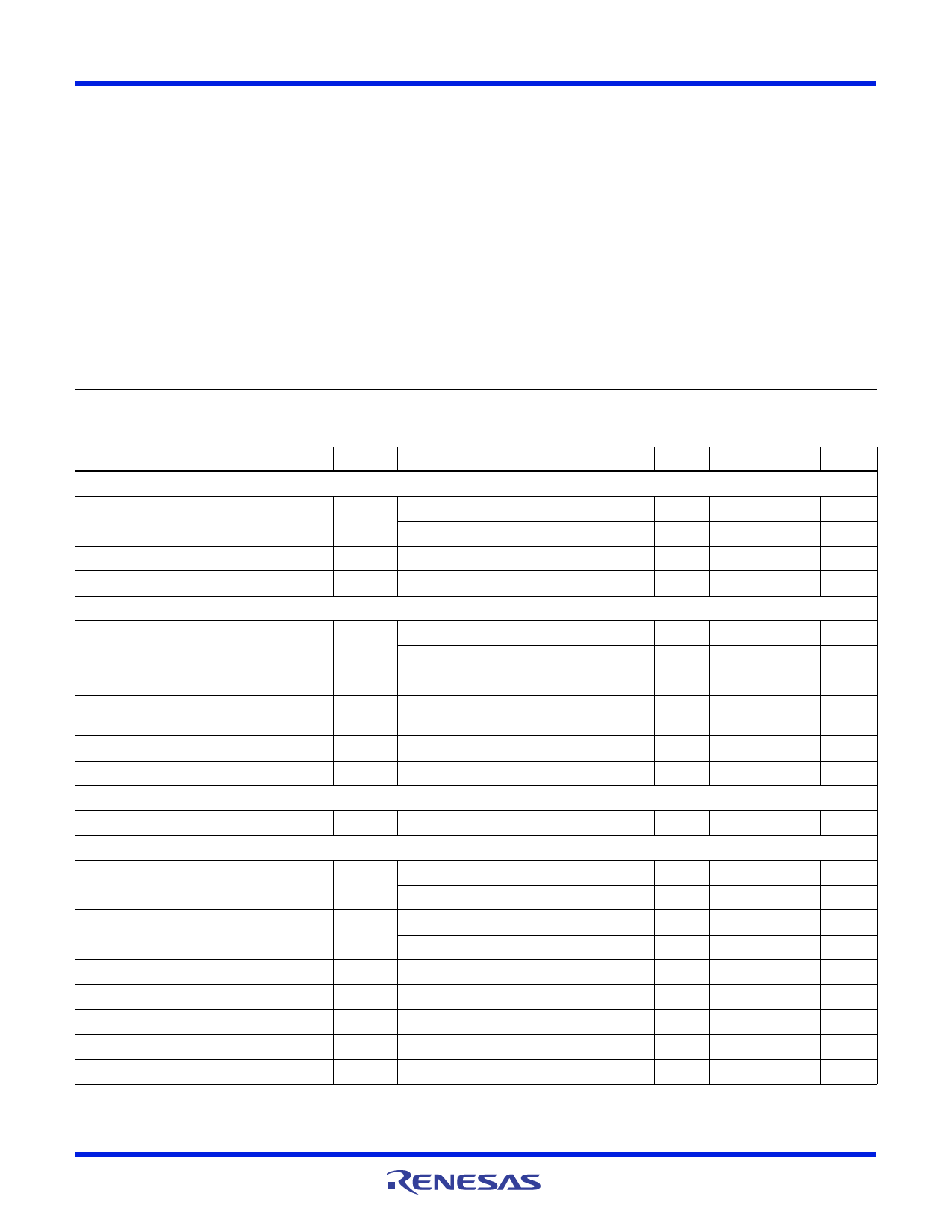
Electrical Specifications
TA = +25°C, VPVIN = VVCC = 3.6V, EN = VCC, L = 1.8µH, C1 = 10µF, C2 = 10µF, IOUT = 0A (see “Typical
Applications” on page 6); Parameters with MIN and/or MAX limits are 100% tested at +25°C, unless otherwise
specified. Temperature limits established by characterization and are not production tested.
PARAMETER
SYMBOL
TEST CONDITIONS
MIN
TYP
MAX UNITS
SUPPLY
VCC Undervoltage Lockout Threshold
VUVLO Rising
Falling
-
2.5
2.7
V
2.2
2.4
-
V
Quiescent Supply Current
Shut Down Supply Current
OUTPUT REGULATION
IPVIN
ISD
No load at the output
VCC = PVIN = 5.5V, EN = low
-
5
8
mA
-
0.1
2
µA
FB Regulation Voltage
FB Bias Current
Output Voltage Accuracy
Line Regulation
Maximum Output Current
VFB TA = 0°C to +85°C
0.784
0.8
0.816
V
TA = -40°C to +85°C
0.78
0.8
0.82
V
IFB FB = 0.75V
-
0.1
-
µA
PVIN = VO + 0.5V to 5.5V, IO = 0A to 1.2A,
-3
-
3
%
TA = -40°C to +85°C
PVIN = VO + 0.5V to 5.5V (minimal 2.7V)
-
0.2
-
%/V
1.2
-
-
A
COMPENSATION
Error Amplifier Trans-conductance
Adjustable version, design info only
-
20
-
µA/V
PHASE
P-Channel MOSFET On-Resistance
N-Channel MOSFET On-Resistance
P-Channel MOSFET Peak Current Limit
PHASE Maximum Duty Cycle
PVIN = 3.6V, IO = 200mA
PVIN = 2.7V, IO = 200mA
PVIN = 3.6V, IO = 200mA
PVIN = 2.7V, IO = 200mA
IPK
-
0.12 0.22
-
0.16 0.27
-
0.11
0.22
-
0.15 0.27
1.5
2.1
2.6
A
-
100
-
%
PWM Switching Frequency
PHASE Minimum On Time
fS
TA = -40°C to +85°C
1.35
1.6
1.75
MHz
-
-
140
ns
Soft Start-Up Time
-
1.1
-
ms
FN9254 Rev 2.00
August 4, 2009
Page 2 of 10
Share Link: 