ISL8011 データシートの表示(PDF) - Renesas Electronics
部品番号
コンポーネント説明
メーカー
ISL8011 Datasheet PDF : 10 Pages
| |||
ISL8011
Theory of Operation
ISL8011 is an integrated FET, 1.2A synchronous buck
regulator for general purpose point-of load applications. The
regulator operates at 1.5MHz fixed switching frequency
under heavy load condition to allow small external inductor
and capacitors to be used for minimal printed-circuit board
(PCB) area. The supply current is typically only 0.1µA when
the regulator is shut down.
PWM Control Scheme
The ISL8011 employs the current-mode pulse-width
modulation (PWM) control scheme for fast transient
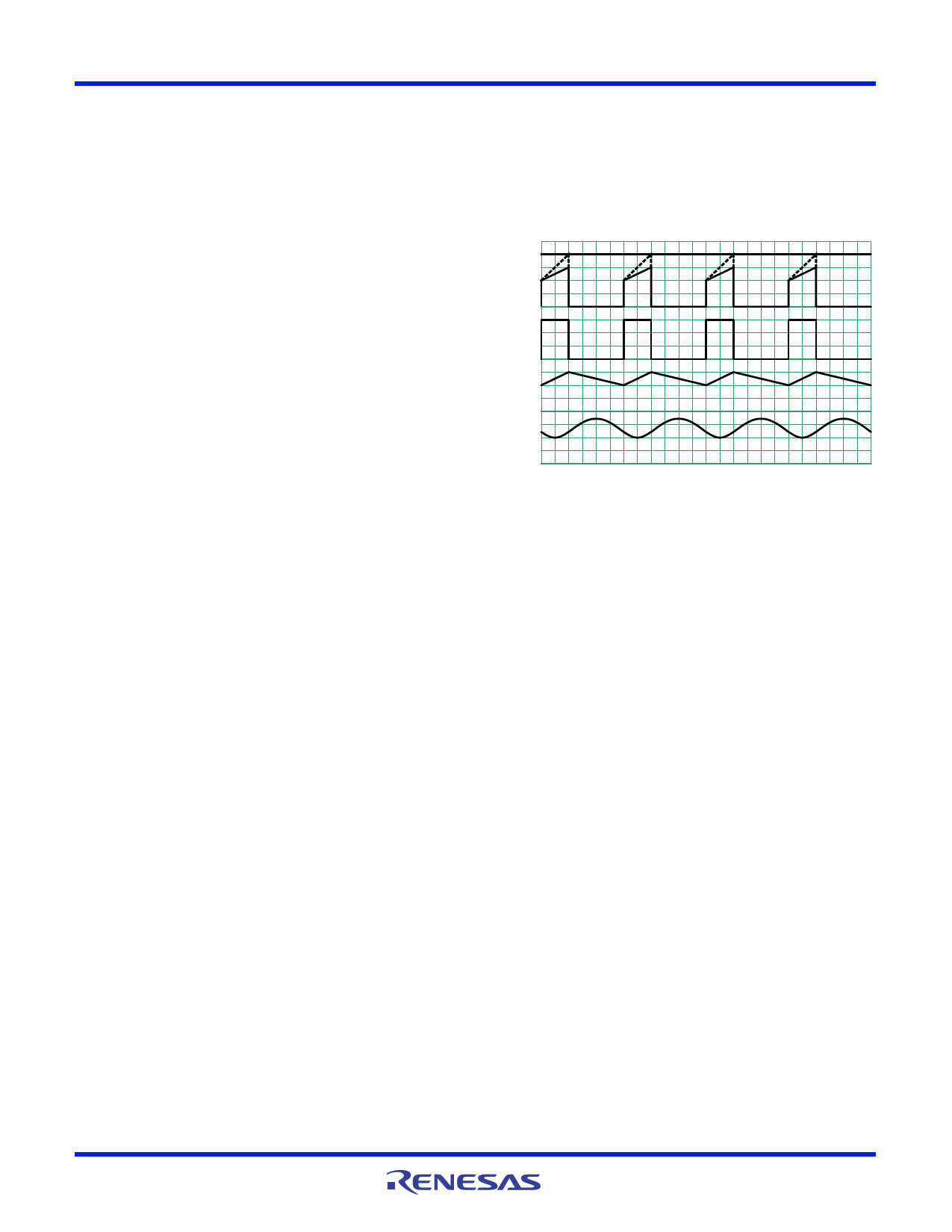
response and pulse-by-pulse current limiting. Figure 11
shows the block diagram. The current loop consists of the
oscillator, the PWM comparator COMP, current sensing
circuit, and the slope compensation for the current loop
stability. The current sensing circuit consists of the
resistance of the P-Channel MOSFET when it is turned on
and the current sense amplifier (CSA1). The gain for the
current sensing circuit is typically 0.4V/A. The control
reference for the current loops comes from the error
amplifier EAMP of the voltage loop.
The PWM operation is initialized by the clock from the
oscillator. The P-Channel MOSFET is turned on at the
beginning of a PWM cycle and the current in the MOSFET
starts to ramp up. When the sum of the CSA1 and the
compensation slope (0.675V/µs) reaches the control
reference of the current loop, the PWM comparator COMP
sends a signal to the PWM logic to turn off the P-MOSFET
and to turn on the N-Channel MOSFET. The N-MOSFET
stays on until the end of the PWM cycle. Figure 12 shows
the typical operating waveforms during the PWM operation.
The dotted lines illustrate the sum of the compensation ramp
and the CSA1 output.
The output voltage is regulated by controlling the reference
voltage to the current loop. The bandgap circuit outputs a
0.8V reference voltage to the voltage control loop. The
feedback signal comes from the FB pin. The soft-start block
only affects the operation during the start-up and will be
discussed separately shortly. The error amplifier is a
transconductance amplifier that converts the voltage error
signal to a current output. The voltage loop is internally
compensated with the 25pF and 400k RC network. The
maximum EAMP voltage output is precisely clamped to the
bandgap voltage (1.172V).
Overcurrent Protection
The overcurrent protection is realized by monitoring the
CSA1 output with the OCP comparator, as shown in
Figure 11. The current sensing circuit has a gain of 0.4V/A,
from the N-MOSFET current to the CSA1 output. When the
CSA1 output reaches 1V, which is equivalent to 2.5A for the
switch current, the OCP comparator is tripped to turn off the
P-MOSFET immediately.
FN9254 Rev 2.00
August 4, 2009
Short-Circuit Protection
A short-circuit protection (SCP) comparator monitors the FB
pin voltage for output short-circuit protection. When the FB is
lower than 0.2V, the SCP comparator forces the PWM
oscillator frequency to drop to 1/3 of the normal operation
value. This comparator is effective during start-up or an
output short-circuit event.
VEAMP
VCSA1
Duty
Cycle
IL
VOUT
FIGURE 12. PWM OPERATION WAVEFORMS
POR Signal
The ISL8011 offers a power-on reset (POR) signal for
resetting the microprocessor at the power-up. When the
output voltage is not within a power-good window, the POR
pin outputs an open-drain low signal to reset the
microprocessor. The output voltage is monitored through the
FB pin. When the voltage of the monitored node is within the
window of 0.736V and 0.864V, a power-good signal is issued
to turn off the open-drain POR pin. The rising edge of the
POR output is delayed by 200ms.
UVLO
When the input voltage is below the undervoltage lock out
(UVLO) threshold, the regulator is disabled.
Soft Start-Up
The soft start-up eliminates the inrush current during the
start-up. The soft-start block outputs a ramp reference to
both the voltage loop and the current loop. The two ramps
limit the inductor current rising speed as well as the output
voltage speed so that the output voltage rises in a controlled
fashion. At the very beginning of the start-up, the output
voltage is less than 0.2V; hence the PWM operating
frequency is 1/3 of the normal frequency. Figure 7 shows the
start-up waveforms.
Power MOSFETs
The power MOSFETs are optimized for best efficiency. The
ON-resistance for the P-MOSFET is typically 150m and
the ON-resistance for the N-MOSFET is typically 150m.
100% Duty Cycle
The ISL8011 features 100% duty cycle operation to
maximize the battery life. When the battery voltage drops to
Page 7 of 10
Share Link: 