5164ISZ データシートの表示(PDF) - Renesas Electronics
部品番号
コンポーネント説明
メーカー
5164ISZ Datasheet PDF : 17 Pages
| |||
EL5164, EL5165, EL5364
Output Drive Capability
In spite of their low 3.5mA of supply current, the EL5164, EL5165,
and EL5364 are capable of providing a minimum of ±100mA of
output current. With a minimum of ±100mA of output drive, the
EL5164, EL5165, and EL5364 are capable of driving 50 loads to
both rails, making it an excellent choice for driving isolation
transformers in telecommunications applications.
Driving Cables and Capacitive Loads
When used as a cable driver, double termination is always
recommended for reflection-free performance. For those
applications, the back-termination series resistor will decouple
the EL5164, EL5165, and EL5364 from the cable and allow
extensive capacitive drive. However, other applications may have
high capacitive loads without a back-termination resistor. In
these applications, a small resistor (usually between 5 and
50) can be placed in series with the output to eliminate most
peaking. The gain resistor (RG) can then be chosen to make up
for any gain loss which may be created by this additional resistor
at the output. In many cases it is also possible to simply increase
the value of the feedback resistor (RF) to reduce the peaking.
Current Limiting
The EL5164, EL5165, and EL5364 have no internal output
current-limiting circuitry. If the output is shorted, it is possible to
exceed the Absolute Maximum Rating for output current or
power dissipation, potentially resulting in the destruction of the
device.
Power Dissipation
With the high output drive capability of the EL5164, EL5165, and
EL5364, it is possible to exceed the +125°C Absolute Maximum
junction temperature under certain very high load current
conditions. Generally speaking when RL falls below about 25, it
is important to calculate the maximum junction temperature
(TJMAX) for the application, to determine if power supply voltages,
load conditions, or package type need to be modified to remain
in the safe operating area. These parameters are calculated in
Equation 1:
TJMAX = TMAX + JA n PDMAX
(EQ. 1)
where:
• TMAX = Maximum ambient temperature
• JA = Thermal resistance of the package
• n = Number of amplifiers in the package
• PDMAX = Maximum power dissipation of each amplifier in the
package
PDMAX for each amplifier can be calculated in Equation 2:
PDMAX = 2 VS ISMAX + VS – VOUTMAX V-----O----U--R--T---L-M-----A----X--
(EQ. 2)
where:
• VS = Supply voltage
• ISMAX = Maximum supply current of 4.2mA
• VOUTMAX = Maximum output voltage (required)
• RL = Load resistance
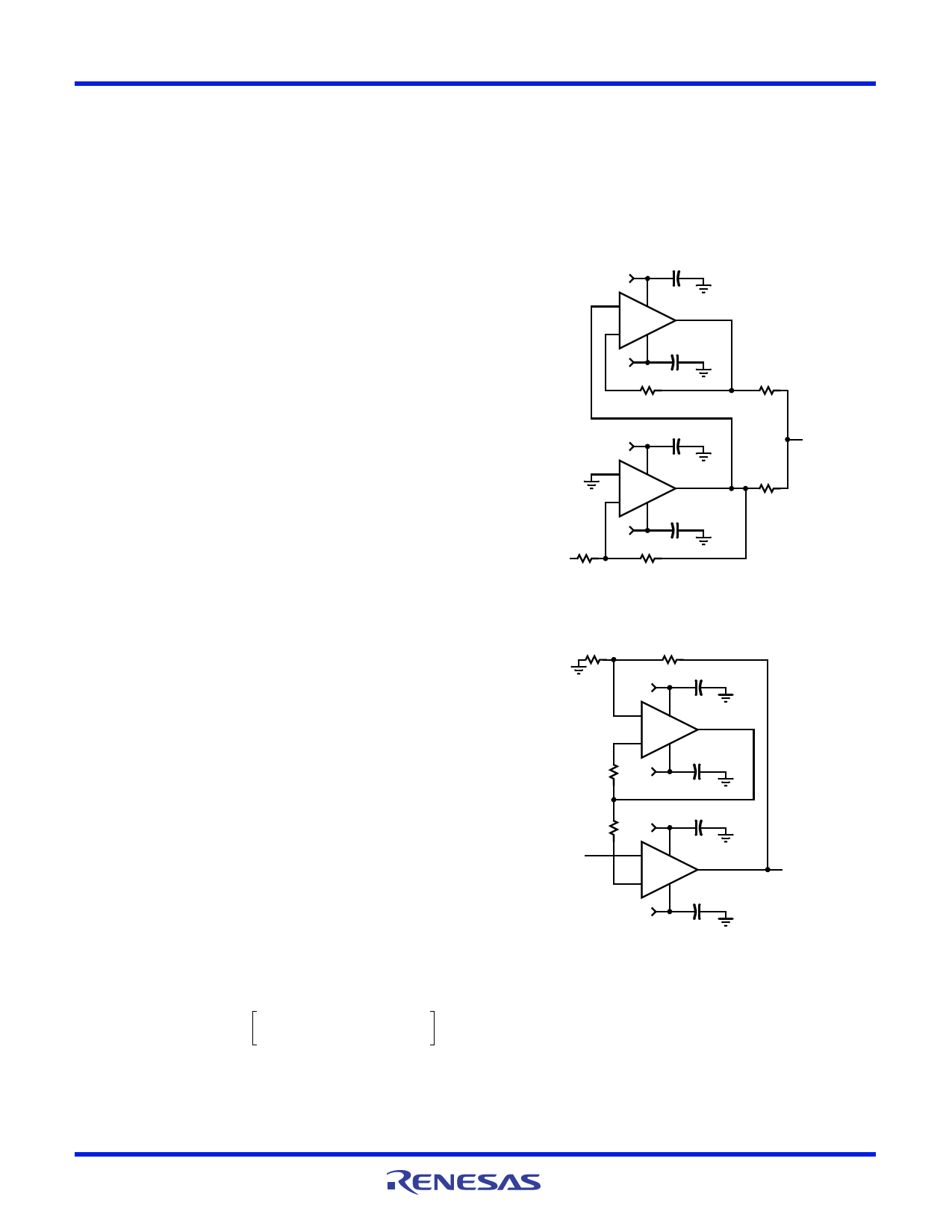
Typical Application Circuits
0.1µF
+5V
IN+
IN-
-5V
VS+ OUT
VS-
0.1µF
375
5
0.1µF
+5V
IN+
IN-
-5V
VS+ OUT
VS-
0.1µF
375
VIN
375
VOUT
5
FIGURE 24. INVERTING 200mA OUTPUT CURRENT DISTRIBUTION
AMPLIFIER
375
375
+5V
IN+
IN-
375 -5V
0.1µF
VS+ OUT
VS-
0.1µF
375
VIN
+5V
IN+
IN-
-5V
0.1µF
VS+ OUT
VS-
0.1µF
VOUT
FIGURE 25. FAST-SETTLING PRECISION AMPLIFIER
FN7389 Rev 9.00
January 30, 2014
Page 11 of 17
Share Link: 