5164ISZ データシートの表示(PDF) - Renesas Electronics
部品番号
コンポーネント説明
メーカー
5164ISZ Datasheet PDF : 17 Pages
| |||
EL5164, EL5165, EL5364
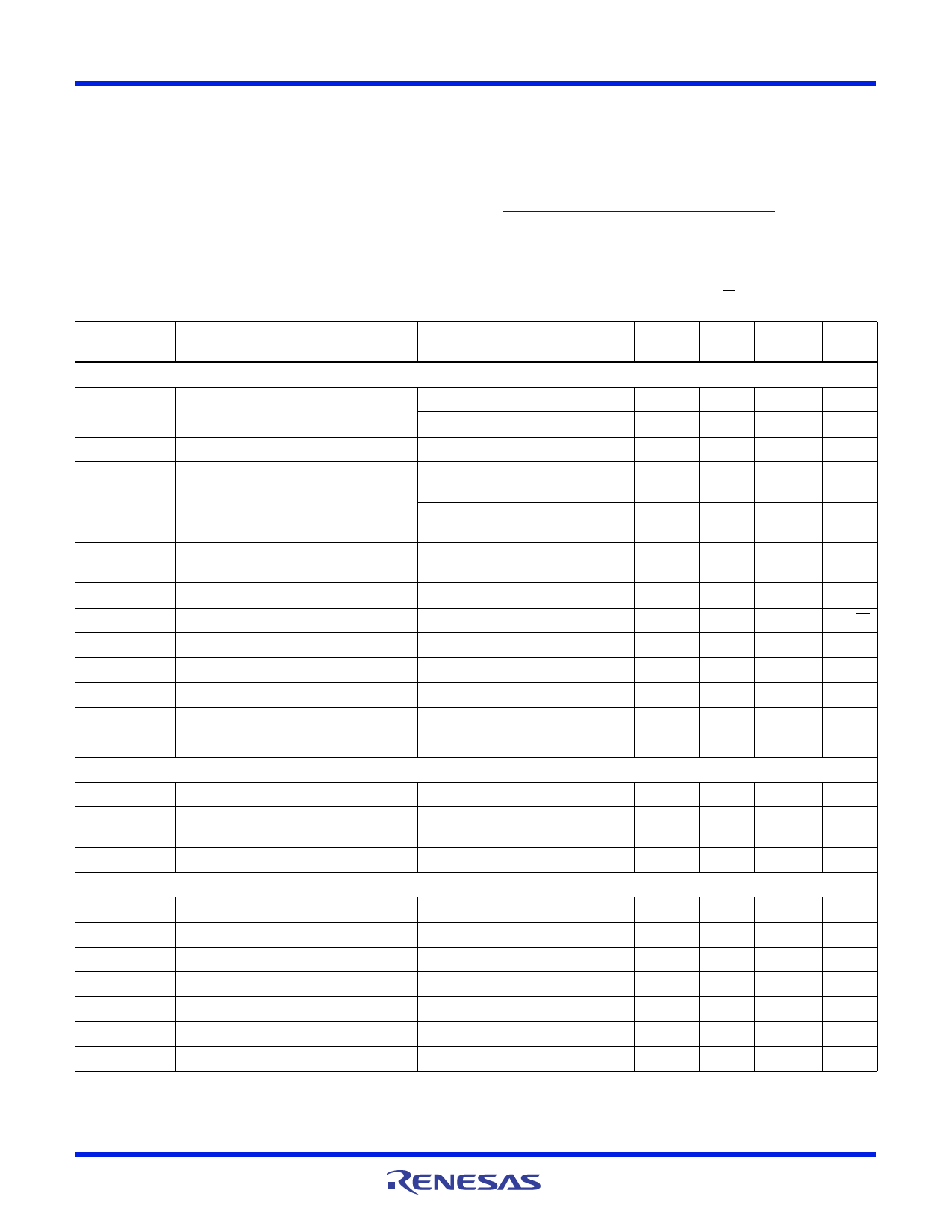
Absolute Maximum Ratings (TA = +25°C)
Supply Voltage between VS+ and VS-. . . . . . . . . . . . . . . . . . . . . . . . . . 13.2V
Maximum Continuous Output Current . . . . . . . . . . . . . . . . . . . . . . . . . 50mA
Pin Voltages. . . . . . . . . . . . . . . . . . . . . . . . . . . . . (VS-) - 0.5V to (VS+) + 0.5V
Supply Slewrate between VS+ and VS-. . . . . . . . . . . . . . . . . . . . 1V/µs(Max)
VIN-DIFF (VIN+ - VIN-) (When Disabled) . . . . . . . . . . . . . . . . . . . . . . ±2V (Max)
Thermal Information
Maximum Power Dissipation . . . . . . . . . . . . . . . . . . . see curves on page 8
Maximum Storage Temperature Range . . . . . . . . . . . . . -65°C to +150°C
Ambient Operating Temperature Range . . . . . . . . . . . . . . -40°C to +85°C
Maximum Operating Junction Temperature . . . . . . . . . . . . . . . . . . +125°C
Pb-free reflow profile . . . . . . . . . . . . . . . . . . . . . . . . . . . . . . . . see link below
http://www.intersil.com/pbfree/Pb-FreeReflow.asp
CAUTION: Do not operate at or near the maximum ratings listed for extended periods of time. Exposure to such conditions may adversely impact product
reliability and result in failures not covered by warranty
Electrical Specifications VS+ = +5V, VS- = -5V, RF = 750 for AV = 1, RF = 375 for AV = 2, RL = 150, VCE = 0V, TA = +25°C unless
otherwise specified. Boldface limits apply across the operating temperature range, -40°C to +85°C.
PARAMETER
DESCRIPTION
CONDITIONS
MIN
MAX
(Note 6) Typ (Note 6) UNIT
AC PERFORMANCE
BW
BW1
SR
-3dB Bandwidth
0.1dB Bandwidth
Slew Rate
AV = +1, RL = 500RF = 510
AV = +2, RL = 150RF = 412
AV = +2, RL = 150RF = 412
VOUT = -3V to +3V, AV = +2, RL = 100
(EL5164, EL5165)
3500
600
450
50
4700
7000
MHz
MHz
MHz
V/µs
VOUT = -3V to +3V, AV = +2, RL = 100 3000
(EL5364)
4200
6000
V/µs
tS
0.1% Settling Time
eN
Input Voltage Noise
iN-
IN- Input Current Noise
iN+
IN+ Input Current Noise
HD2
HD3
dG
Differential Gain Error (Note 5)
dP
Differential Phase Error (Note 5)
DC PERFORMANCE
VOUT = -2.5V to +2.5V, AV = +2,
RF = RG = 1k
f = 1MHz
f = 1MHz
f = 1MHz
5MHz, 2.5VP-P
5MHz, 2.5VP-P
AV = +2
AV = +2
15
ns
2.1
nV/Hz
13
pA/Hz
13
pA/Hz
-81
dBc
-74
dBc
0.01
%
0.01
°
VOS
TCVOS
Offset Voltage
Input Offset Voltage Temperature
Coefficient
Measured from TMIN to TMAX
-5
1.5
+5
mV
6
µV/°C
ROL
Open Loop Transimpedance Gain
INPUT CHARACTERISTICS
1.1
3
M
CMIR
Common Mode Input Range
Guaranteed by CMRR test
±3
±3.3
V
CMRR
-ICMR
Common Mode Rejection Ratio
- Input Current Common Mode Rejection
VIN = ±3V
50
62
75
dB
-1
0.1
+1
µA/V
+IIN
+ Input Current
-IIN
- Input Current
RIN
Input Resistance
CIN
Input Capacitance
+ Input
-10
2
+10
µA
-10
2
+10
µA
300
650
1200
k
1
pF
FN7389 Rev 9.00
January 30, 2014
Page 3 of 17
Share Link: 