ICM7243 データシートの表示(PDF) - Renesas Electronics
部品番号
コンポーネント説明
メーカー
ICM7243 Datasheet PDF : 17 Pages
| |||
ICM7243
Absolute Maximum Ratings
Thermal Information
Supply Voltage VDD - VSS . . . . . . . . . . . . . . . . . . . . . . . . . . . . +6.0V
Input Voltage (Any Terminal) . . . . . . . . . . VDD + 0.3V to VSS - 0.3V
CHARacter Output Current . . . . . . . . . . . . . . . . . . . . . . . . . . 300mA
SEGment Output Current. . . . . . . . . . . . . . . . . . . . . . . . . . . . . 30mA
Operating Conditions
Temperature Range . . . . . . . . . . . . . . . . . . . . . . . . . .-25°C to +85°C
Thermal Resistance (Typical, Note 1)
qJA (°C/W) qJC (°C/W)
PDIP Package . . . . . . . . . . . . . . . . . . .
50
N/A
MQFP Package . . . . . . . . . . . . . . . . . .
70
N/A
Maximum Junction Temperature . . . . . . . . . . . . . . . . . . . . . . +150°C
Maximum Storage Temperature Range . . . . . . . . . .-65°C to +150°C
Pb-Free Reflow Profile. . . . . . . . . . . . . . . . . . . . . . . . .see link below
http://www.intersil.com/pbfree/Pb-FreeReflow.asp
*Pb-free PDIPs can be used for through hole wave solder
processing only. They are not intended for use in Reflow solder
processing applications.
CAUTION: Do not operate at or near the maximum ratings listed for extended periods of time. Exposure to such conditions may adversely impact product reliability and
result in failures not covered by warranty.
NOTES:
1. JA is measured with the component mounted on an evaluation PC board in free air.
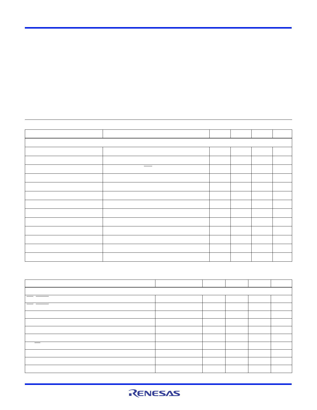
Electrical Specifications VDD = 5V, VSS = 0V, TA = +25°C, Unless Otherwise Specified.
PARAMETER
TEST CONDITIONS
MIN
TYP
MAX UNITS
DC CHARACTERISTICS
Supply Voltage (VDD - VSS), VSUPP
Operating Supply Current, IDD
Quiescent Supply Current, ISTBY
Input High Voltage, VIH
Input Low Voltage, VIL
Input Current, IIN
CHARacter Drive Current, ICHAR
CHARacter Leakage Current, ICHLK
SEGment Drive Current, ISEG
SEGment Leakage Current, ISLK
DISPlay FULL Output Low, VOL
DISPlay FULL Output High, VOH
Display Scan Rate, fDS
VSUPP = 5.25V, 10 Segments ON, All 8 Characters
VSUPP = 5.25V, OSC/OFF Pin < 0.5V, CS = VSS
VSUPP = 5V, VOUT = 1V
VSUPP = 5V, VOUT = 2.5V
IOL = 1.6mA
lIH = 100µA
4.75
5.0
5.25
V
-
180
-
mA
-
30
250
µA
2
-
-
V
-
-
0.8
V
-10
-
+10
µA
140
190
-
mA
-
-
100
µA
14
19
-
mA
-
0.01
10
µA
-
-
0.4
V
2.4
-
-
V
-
400
-
Hz
Electrical Specifications Drive levels 0.4V and 2.4V, timing measured at 0.8V and 2.0V. VDD = 5V, TA = +25°C,
Unless Otherwise Specified.
PARAMETER
TEST CONDITIONS
MIN
TYP
AC CHARACTERISTICS
WR, CLeaR Pulse Width Low, tWPI
WR, CLeaR Pulse Width High (Note 1), tWPH
Data Hold Time, tDH
Data Setup Time, tDS
Address Hold Time, tAH
Address Setup Time, tAS
CS, CS Setup Time, tCS
Pulse Transition Time, tT
SEN Setup Time, tSEN
Display Full Delay, tWDF
300
250
-
250
0
-100
250
150
125
-
40
15
0
-
-
-
0
-25
700
480
MAX
-
-
-
-
-
-
-
100
-
-
UNITS
ns
ns
ns
ns
ns
ns
ns
ns
ns
ns
FN3162 Rev 5.00
October 2, 2015
Page 5 of 17
Share Link: 