CY7C197N データシートの表示(PDF) - Cypress Semiconductor
部品番号
コンポーネント説明
メーカー
CY7C197N Datasheet PDF : 7 Pages
| |||
CY7C197N
Maximum Ratings
(Above which the useful life may be impaired. For user guide-
lines, not tested.)
Storage Temperature ................................. –65°C to +150°C
Ambient Temperature with
Power Applied............................................. –55°C to +125°C
Supply Voltage to Ground Potential
(Pin 24 to Pin 12) ........................................... –0.5V to +7.0V
DC Voltage Applied to Outputs
in High Z State[1] ....................................–0.5V to VCC + 0.5V
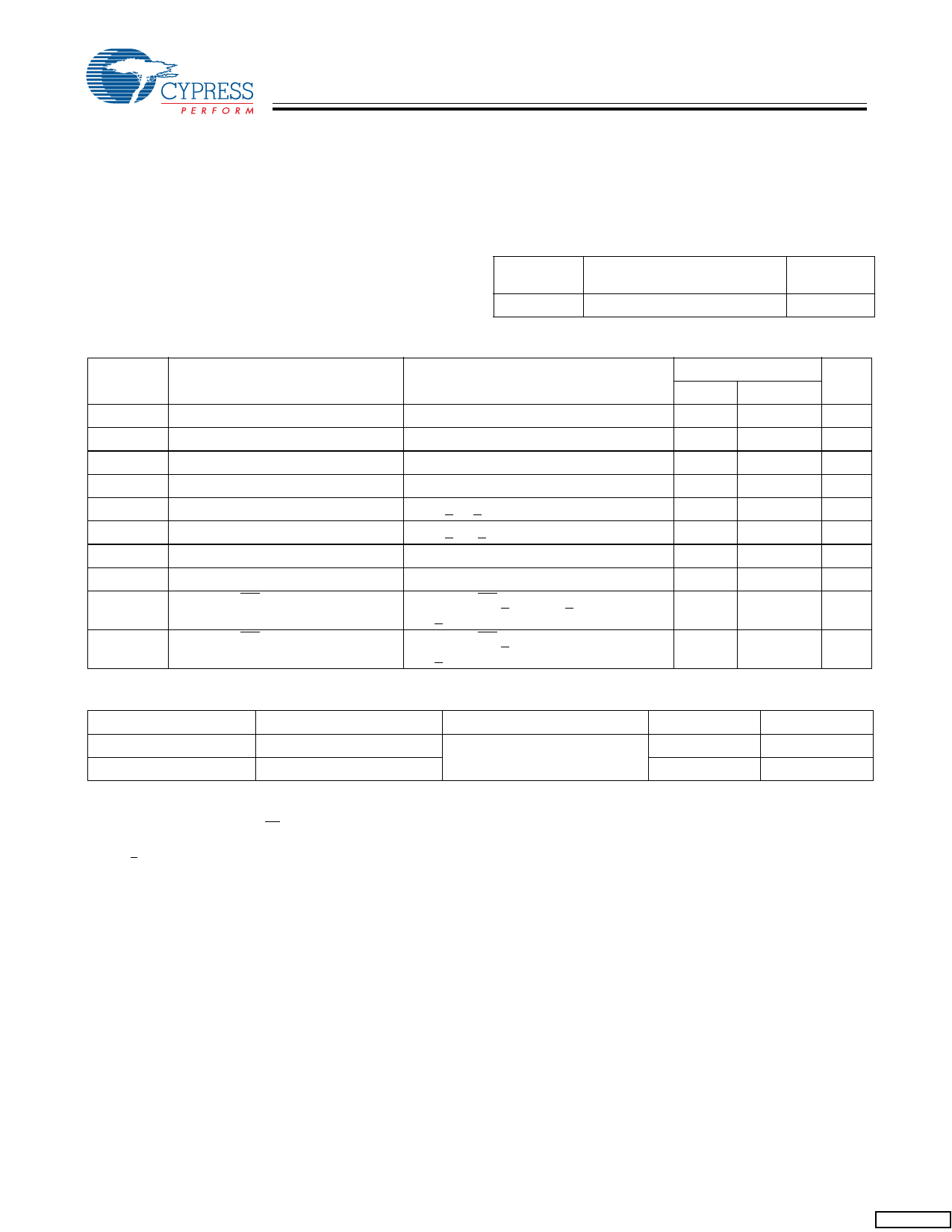
Electrical Characteristics Over the Operating Range
DC Input Voltage[1] ................................ –0.5V to VCC + 0.5V
Output Current into Outputs (LOW)............................. 20 mA
Static Discharge Voltage........................................... >2001V
(per MIL-STD-883, Method 3015)
Latch-Up Current .................................................... >200 mA
Operating Range
Range
Commercial
Ambient Temperature
0°C to +70°C
VCC
5V ± 10%
Parameter
Description
VOH
Output HIGH Voltage
VOL
Output LOW Voltage
VIH
Input HIGH Voltage
VIL
Input LOW Voltage[1]
IIX
Input Load Current
IOZ
Output Leakage Current
IOS
Output Short Circuit Current[2]
ICC
VCC Operating Supply Current
ISB1
Automatic CE Power-Down
Current—TTL Inputs[3]
ISB2
Automatic CE Power-Down
Current—CMOS Inputs[3]
Test Conditions
VCC = Min., IOH = –4.0 mA
VCC = Min., IOL=12.0 mA
GND < VI < VCC
GND < VO < VCC, Output Disabled
VCC = Max., VOUT = GND
VCC = Max., IOUT = 0 mA, f = fMAX = 1/tRC
Max. VCC, CE > VIH, VIN > VIH or
VIN < VIL, f = fMAX
Max. VCC, CE > VCC – 0.3V,
VIN > VCC – 0.3V or VIN < 0.3V
-25, -45
Min.
Max.
Unit
2.4
V
0.4
V
2.2 VCC + 0.3V V
–0.5
0.8
V
–5
+5
mA
–5
+5
mA
-300
mA
95
mA
30
mA
15
mA
Capacitance[4]
Parameter
Description
Test Conditions
Max.
Unit
CIN
COUT
Input Capacitance
Output Capacitance
TA = 25°C, f = 1 MHz,
VCC = 5.0V
8
pF
10
pF
Note:
1. V(min.) = -2.0V for pulse durations of less than 20 ns.
2. Not more than one output should be shorted at one time. Duration of the short circuit should not exceed 30 seconds.
3. A pull-up resistor to VCC on the CE input is required to keep the device deselected during VCC power-up, otherwise ISB will exceed values given.
4. Tested initially and after any design or process changes that may affect these parameters.
5. tr = < 5 ns for the -25 and slower speeds.
Document #: 001-06495 Rev. **
Page 2 of 7
[+] Feedback
Share Link: 