SS34 データシートの表示(PDF) - Jinan Jing Heng Electronics Co., Ltd.
部品番号
コンポーネント説明
メーカー
SS34 Datasheet PDF : 2 Pages
| |||
R
SEMICONDUCTOR
SS32 THRU SS320
SCHOTTKY BARRIER RECTIFIER
Reverse Voltage - 20 to 200 Volts
Forward Current - 3.0Amperes
FEATURES
Plastic package has Underwriters Laboratory
Flammability Classification 94V-0
Metal silicon junction ,majority carrier conduction
For surface mount applications
Low power loss ,high efficiency
High current capability ,Low forward voltage drop
Low profile package
built-in strain relief ,ideal for automated placement
For use in low voltage ,high frequency inverters,
free wheeling ,and polarity protection applications
High temperature soldering guaranteed:260°C/10 seconds at terminals
Component in accordance to RoHS 2011/65/EU
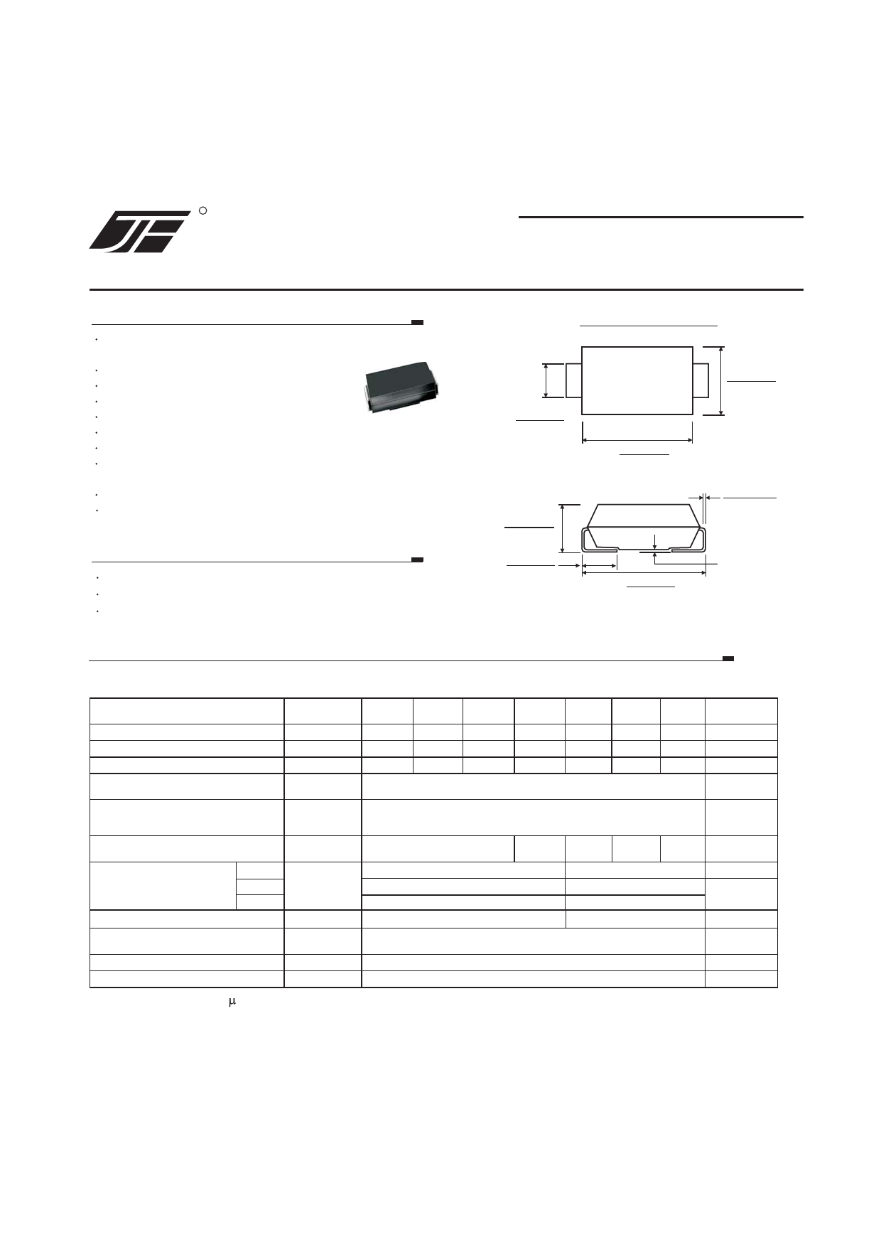
MECHANICAL DATA
Case: JEDEC SMA(DO-214AC) molded plastic body
Terminals: solder plated ,solderable per MIL-STD-750,method 2026
Polarity: color band denotes cathode end
SMA(DO-214AC)
0.065(1.65)
0.049(1.25)
0.185(4.70)
0.157(3.99)
0.110(2.80)
0.094(2.40)
0.090(2.29)
0.075(1.90)
0.012(0.305)
0.006(0.152)
0.060(1.52)
0.030(0.76)
0.208(5.28)
0.185(4.70)
0.008(0.203)
MAX
Dimensions in inches and (millimeters)
MAXIMUM RATINGS AND ELECTRICAL CHARACTERISTICS
(Ratings at 25°C ambient temperature unless otherwise specified ,Single phase ,half wave ,resistive or inductive
load. For capacitive load,derate by 20%.)
Maximum repetitive peak reverse voltage
Maximum RMS voltage
Maximum DC blocking voltage
Maximum average forward rectified current
0.375"(9.5mm) lead length (See Fig.1)
Peak forward surge current 8.3ms single half
sine-wave superimposed on rated load
(JEDEC method)
Maximum instantaneous forward voltage
at 3.0 A(Note 1 )
Maximum instantaneous reverse
current at rated DC blocking
voltage(Note 1)
TA=25°C
TA=100°C
TA=125°C
Typical junction capacitance(Note 3)
Typical thermal resistance (Note 2)
Operating junction temperature range
Storage temperature range
Symbols
VRRM
VRMS
VDC
I(AV)
IFSM
VF
IR
CJ
RθJA
RθJL
TJ
TSTG
SS
SS
32
33
20
30
14
21
20
30
SS
SS
SS
SS
34
36
310
315
40
60
100
150
28
42
70
105
40
60
100
150
3.0
80.0
0.55
100
5
-
250
0.70
88.0
28.0
-55 to+150
-55 to+150
0.85
0.90
20
-
3
160
SS
320
200
140
200
0.95
Units
Volts
Volts
Volts
Amps
Amps
Volts
μA
mA
PF
°C/W
°C
°C
Notes: 1.Pulse test: 300 s pulse width,1% duty cycle
2. P.C.B. mounted 0.55 X 0.55"(14 X 14mm)copper pad areas
3. Measured at 1MHz and reverse voltage of 4.0volts
JINAN JINGHENG ELECTRONICS CO., LTD.
2-1
HTTP://WWW.JINGHENGGROUP.COM
Share Link: 