MPC2106A データシートの表示(PDF) - Motorola => Freescale
部品番号
コンポーネント説明
メーカー
MPC2106A
Motorola => Freescale

MPC2106A Datasheet PDF : 20 Pages
| |||
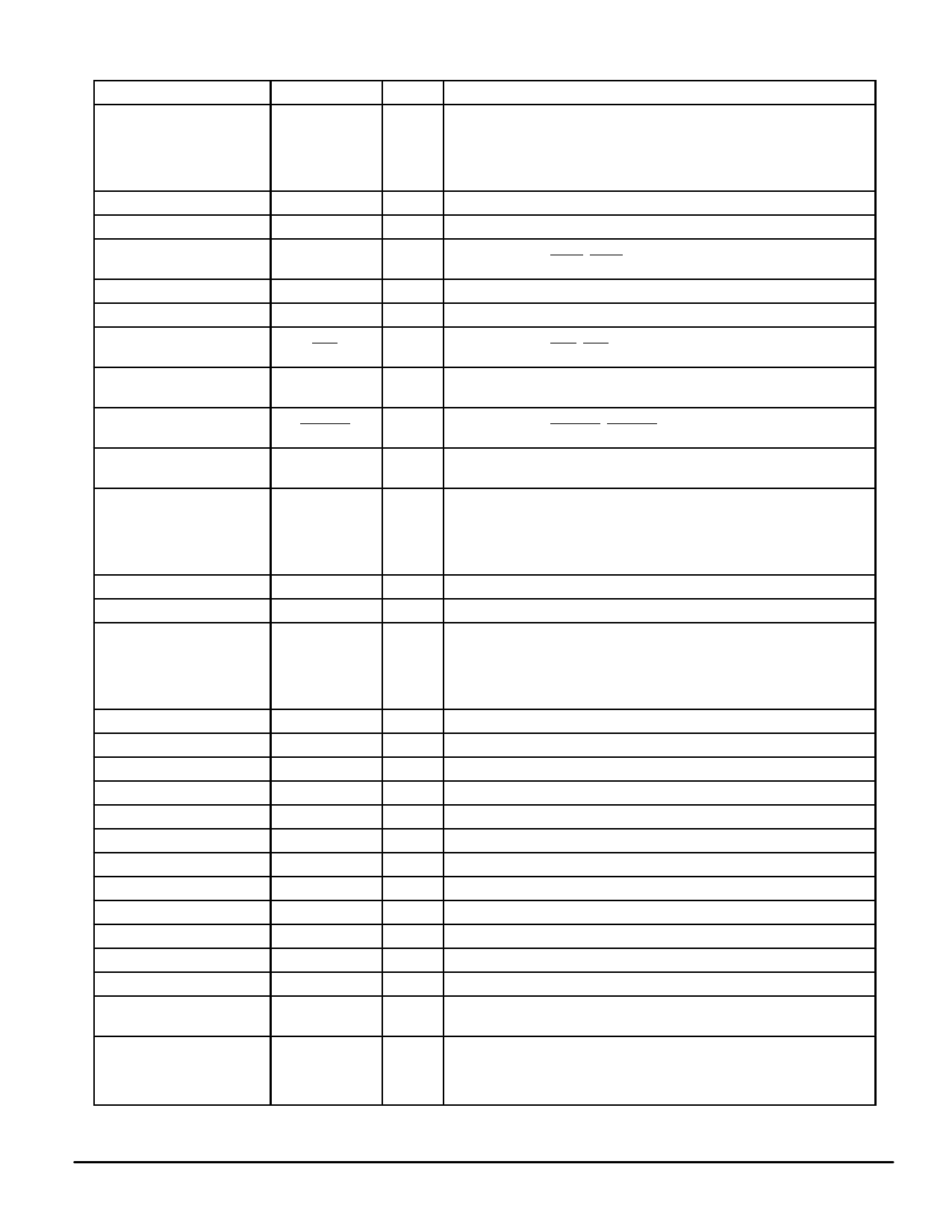
PIN DESCRIPTIONS
Pin Locations
66, 67, 68, 69, 71, 72, 73, 74,
76, 77, 78, 80, 81, 82, 83,
155, 156, 157, 158, 160, 161,
162, 163, 165, 166, 167, 169,
170, 171
62
151
64, 65
Symbol
A0 – A28
ADDR0
ADDR1
ADS0, ADS1
149
172
59, 60
30, 56, 115, 144, 146
ALE
BURSTMODE
CG0,
CG1
CLK0 – CLK4
153, 154
98, 104, 110, 118,
126, 132, 138, 148
4, 5, 6, 7, 10, 11, 12, 14, 16,
17, 19, 20, 22, 24, 25, 26, 27,
93, 94, 95, 96, 99, 100, 101,
103, 105, 106, 108, 109, 111,
113, 117
88
177
32, 33, 34, 37, 38, 39, 40, 43,
44, 45, 47, 49, 50, 52, 53, 54,
119, 120, 122, 123, 124, 127,
128, 129, 131, 133, 134, 136,
137, 139, 141, 142
9, 15, 21, 28, 35, 42, 48, 58
86
2
91
3, 92
63, 152
176
85
87
175
174
18, 36, 84, 107, 125, 173
8, 23, 51, 61, 75, 97, 112,
140, 150, 164
1, 13, 29, 31, 41, 46, 55, 57,
70, 79, 89, 90, 102, 114,
116, 121, 130, 135, 143,
145, 147, 159, 168, 178
CNTEN0,
CNTEN1
CWE0 – CWE7
DH0 – DH31
DIRTYIN
DIRTYOUT
DL0 – DL31
DP0 – DP7
MATCH
PD0/IDSCLK
PD1/IDSDATA
PD2, PD3
RESERVED
STANDBY
TCLR
TG
TWE
VALIDIN
VCC
VDD
VSS
Type
Input
Description
Address Inputs – (MSB:0, LSB:28).
Input
Input
Input
Input
Input
Input
Input
Input
Input
Least significant address bit when asynchronous Data RAMs are used.
Next to least significant address bit when asynchronous Data RAMs are used.
Data RAM Address Strobe – For MPC2105A/B use ADS0 only. For
MPC2106A/B use ADS0, ADS1.
Data RAM Address Latch Enable – Use for asynchronous Data RAM only.
Burstmode. 0 = Linear, 1 = Interleaved.
Data RAM Output Enables – For MPC2105A/B use CG0 only. For
MPC2106A/B use CG0, CG1.
Clock Inputs – CLK2 is for Tag RAM, CLK0, 1, 3, and 4 are for Data RAMs only.
For MPC2106A/B use all the clocks. For MPC2105A/B use CLK0 – CLK2 only.
Data RAM Count Enables – For MPC2105A/B use CNTEN0 only. For
MPC2106A/B use CNTEN0, CNTEN1.
Data RAM Write Enables – (MSB:0, LSB:7).
I/O High Data Bus – (MSB:0, LSB:31).
Input
Output
I/O
Dirty input bit.
Dirty output bit.
Low Data Bus – (MSB:0, LSB:31).
I/O
Output
Input
I/O
Output
Input
Input
Input
Input
Input
Input
Input
Data Parity Bits – (MSB:0, LSB:7)
Tag RAM active high match indication.
Presence detect bit 0/EEPROM serial clock. (EEPROM option only).
Presence detect bit 1/EEPROM serial data. (EEPROM option only).
Presence detect bits.
Reserved pin.
Standby pin. Reduces standby power consumption.
Tag RAM clear.
Tag RAM output enable.
Tag RAM write enable.
Tag RAM valid bit.
+ 5 V power supply. Must be connected.
+ 3.3 V power supply. Must be connected.
Input Ground.
MOTOROLA FAST SRAM
MPC2105A•MPC2106A•MPC2105B•MPC2106B
5
Share Link: