VN610SP データシートの表示(PDF) - STMicroelectronics
部品番号
コンポーネント説明
メーカー
VN610SP Datasheet PDF : 17 Pages
| |||
VN610SP
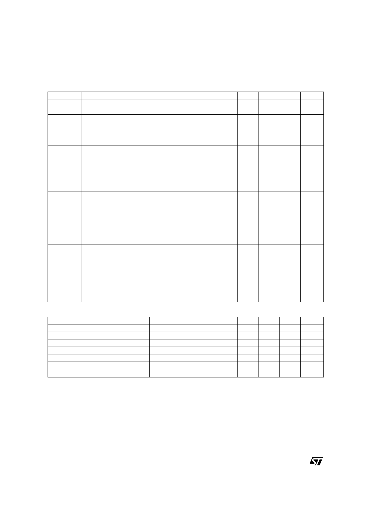
ELECTRICAL CHARACTERISTICS (continued)
CURRENT SENSE (9V≤VCC≤16V) (See Figure 2)
Symbol
K1
dK1/K1
K2
dK2/K2
K3
dK3/K3
ISENSE0
VSENSE
VSENSEH
Parameter
IOUT/ISENSE
Current Sense Ratio Drift
IOUT/ISENSE
Current Sense Ratio Drift
IOUT/ISENSE
Current Sense Ratio Drift
Analog sense current
Max analog sense
output voltage
Analog sense output
voltage in overtemperature
condition
Test Conditions
IOUT=1.5A; VSENSE=0.5V;
Tj= -40°C...150°C
IOUT=1.5A; VSENSE=0.5V;
Tj= -40°C...150°C
IOUT=15A; VSENSE=4V; Tj=-40°C
Tj=25°C...150°C
IOUT=15A; VSENSE=4V; Tj=-40°C
Tj=25°C...150°C
IOUT=45A; VSENSE=4V; Tj=-40°C
Tj=25°C...150°C
IOUT=45A; VSENSE=4V; Tj=-40°C
Tj=25°C...150°C
Vcc=6...16V; IOUT=0A; VSENSE=0V;
Tj=-40°C...150°C
Off State; VIN=0V
On State; VIN=5V
VCC=5.5V; IOUT =7.5A;
RSENSE=10KΩ
VCC >8V; IOUT=15A; RSENSE=10KΩ
VCC=13V; RSENSE=3.9KΩ
RVSENSEH
tDSENSE
Analog sense output
impedance in
overtemperature condition
Current sense delay
reponse
VCC=13V; Tj>TTSD; Output Open
to 90% ISENSE (see note 2)
LOGIC INPUT
Symbol
VIL
IIL
VIH
IIH
VI(hyst)
VICL
Parameter
Input low level voltage
Low level input current
Input high level voltage
High level input current
Input hysteresis voltage
Input clamp voltage
Test Conditions
VIN=1.25V
VIN=3.25V
IIN=1mA
IIN=-1mA
Note 1: Vclamp and VOV are correlated. Typical difference is 5V.
Note 2: current sense signal delay after positive input slope.
Note: Sense pin doesn’t have to be left floating.
Min
3300
-10
4200
4400
-6
4200
4400
-6
0
0
3.5
5
Min
1
3.25
0.5
6
Typ
4400
4900
4900
4900
4900
5.5
400
Typ
6.8
-0.7
Max
6000
+10
6000
5750
+6
5500
5250
+6
5
10
500
Max
1.25
10
8
Unit
%
%
%
µA
µA
V
V
V
Ω
µs
Unit
V
µA
V
µA
V
V
V
4/17
2
Share Link: 