CXP86541 データシートの表示(PDF) - Sony Semiconductor
部品番号
コンポーネント説明
メーカー
CXP86541 Datasheet PDF : 21 Pages
| |||
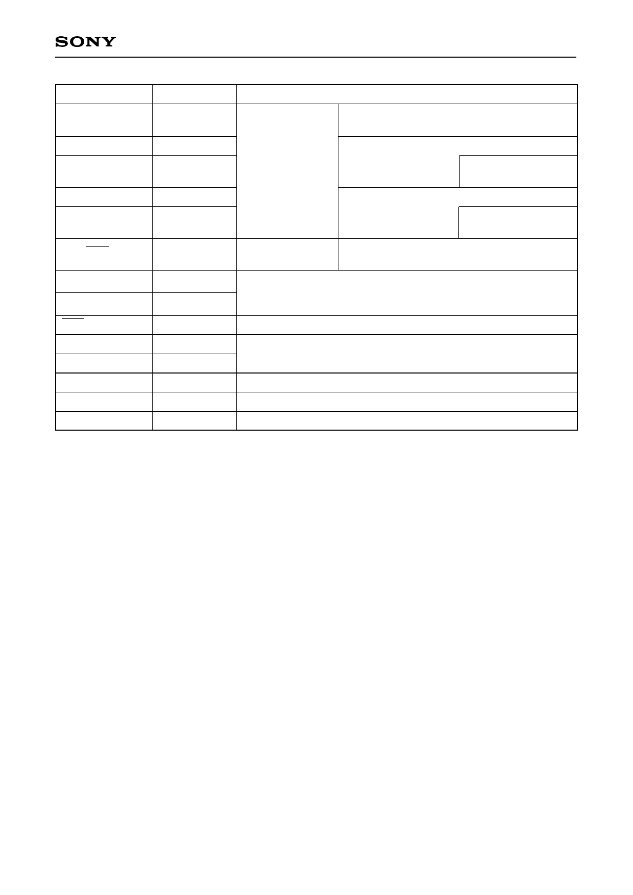
CXP86541/86549/86561
Symbol
PF0/PWM0 to
PF3/PWM3
PF4/SCL0
PF5/SCL1/
PWM4
PF6/SDA0
PF7/SDA1/
PWM5
PG7/INT1
EXTAL
XTAL
RST
EXLC
XLC
NC
VDD
Vss
I/O
Output/Output
Output/I/O
Output/I/O/
Output
Output/I/O
Output/I/O/
Output
I/O/Input
Input
Output
Input
Input
Output
Description
(Port F)
8-bit output port
and large current
(12mA) N-channel
open drain output.
Lower 4 bits are
midium drive voltage
(12V); upper 4 bits
are 5V drive.
(8 pins)
8-bit PWM output.
(4 pins)
I2C bus interface transfer clock I/O.
(2 pins)
8-bit PWM output.
I2C bus interface transfer data I/O.
(2 pins)
8-bit PWM output.
(Port G)
1-bit I/O port.
External interruption request input.
Active at the falling edge.
Connects a crystal for system clock oscillation. When a clock is
supplied externally, input it to EXTAL pin and input a reversed phase
clock to XTAL pin.
System reset; active at Low level.
OSD display clock oscillation I/O. Oscillation frequency is determined
by the external L and C.
No connected.
Positive power supply.
GND. Connect two Vss pins to GND.
–5–
Share Link: 