MRFIC0912 データシートの表示(PDF) - Motorola => Freescale
部品番号
コンポーネント説明
メーカー
MRFIC0912 Datasheet PDF : 6 Pages
| |||
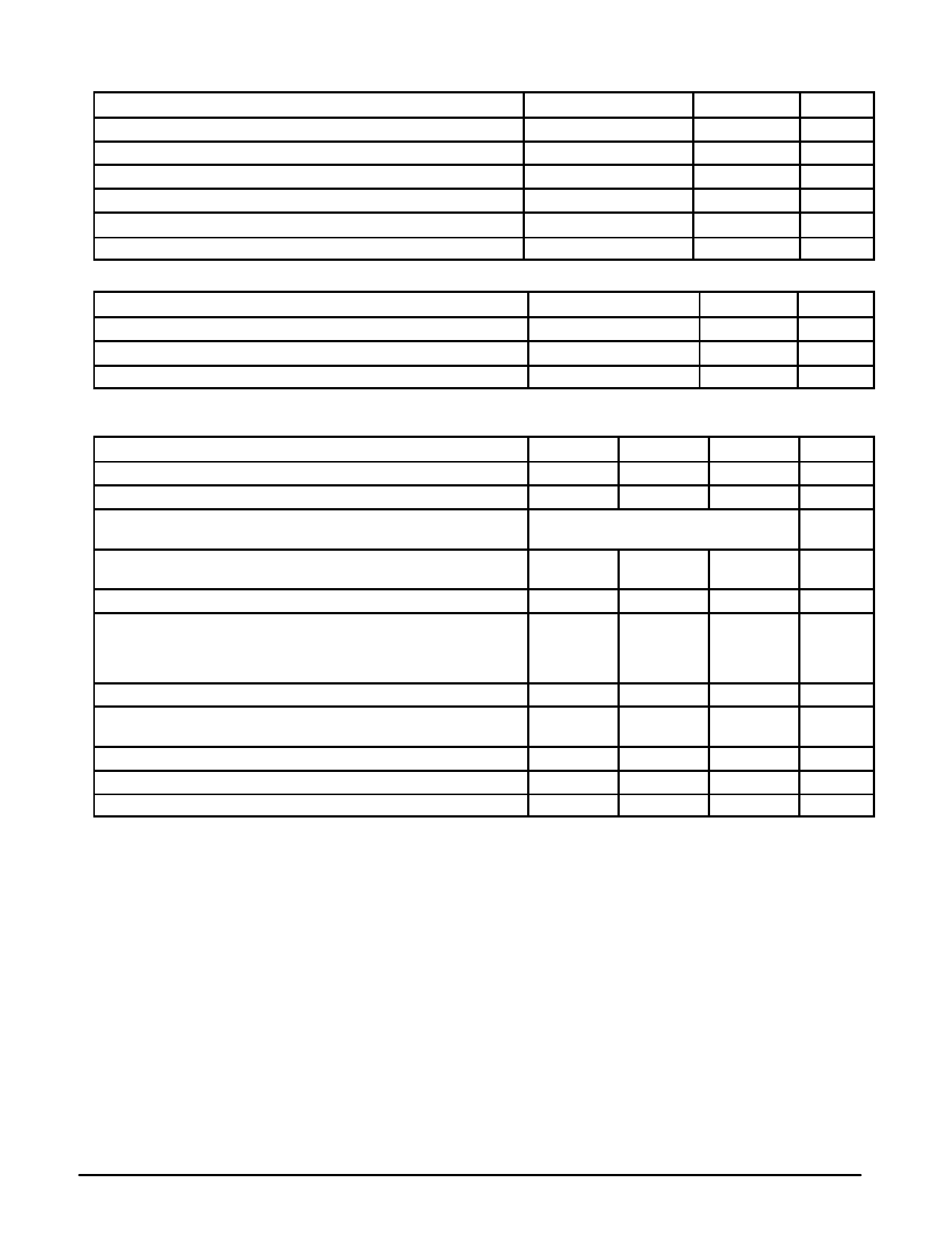
MAXIMUM RATINGS (TA = 25°C unless otherwise noted)
Ratings
Symbol
Limit
Unit
Supply Voltage
RF Input Power
Gate Voltage
Storage Temperature Range
Operating Case Temperature
Thermal Resistance, Junction to Case
VD1, VD2
PRF
VG1, VG2, VGG
Tstg
TC
RθJC
8
20
–5
– 65 to +150
– 35 to +100
18
Vdc
dBm
Vdc
°C
°C
°C/W
RECOMMENDED OPERATING RANGES
Parameter
Symbol
Value
Unit
RF Frequency
Supply Voltage
Gate Voltage
fRF
VD1, VD2
VG1, VG2
824–905
4.0–6.0
–2.3 to –1.5
MHz
Vdc
Vdc
ELECTRICAL CHARACTERISTICS (VD1, VD2 = 4.6 V, TA = 25°C, fRF = 840 MHz, Pin = 7 dBm, VGG set for ID2Q = 200 mA, Tested in
Circuit Shown in Figure 1)
Characteristic
Min
Typ
Max
Unit
RF Output Power
Power Slump (VD1, VD2 = 4.0 V, TC = 100_C)
Load Mismatch Survival (VD1, VD2 = 7 V, Load VSWR = 10:1, all phases,
10 sec)
30.8
31.2
—
28.5
—
—
No Degradation
dBm
dBm
Spurious Output (VD1,VD2 = 0 to 7 V, Pin = 5 to 9 dBm, Load
VSWR = 10:1)
—
—
–60
dBc
Input Return Loss
—
10
—
dB
Harmonic Output (Pout = 30.8 dBm)
2f0
3f0
4f0
dBc
—
—
–25
—
—
–40
—
—
–40
Noise Power (VDD = 0 to 7 V, 45 MHz Above fRF at 30 kHz BW)
—
—
–93
dBm
Maximum Power Control Voltage Slope (Change in Pout for Change on
—
45
—
dB/V
VD1)
Total Supply Current (VD1 set for Pout = 30.8 dBm)
—
430
470
mA
VGG Required for ID2Q = 200 mA
–2.3
–2.0
–1.7
Vdc
Gate Current during RF Operation
–2
—
2
mA
DESIGN AND APPLICATIONS INFORMATION
The MRFIC0912 has been designed for high efficiency
900 MHz applications such as analog cellular and Industrial,
Medical and Scientific (ISM) equipment. The two stage MES-
FET design utilizes Motorola’s planar refractory gate process
to allow high performance GaAs to be applied to consumer
applications. The proprietary PFP–16 package assures good
grounding and low thermal resistance.
As shown in Figure 1, the gate voltage pins can be ganged
together and one voltage applied to both gates to set the
quiescent operating current. Alternatively, VG1 and VG2 can
be set separately. VD1 can be used as power control with a
45 dB per volt sensitivity. The placement of C3 in the VD1
supply line can be varied to optimize RF performance since
T2 is part of a shunt L matching section. On the output, pins
11, 12 and 13, the placement of C11 is adjusted for best RF
performance.
Layout is important for amplifier stability and RF perfor-
mance. Ground vias must be located as close to circuit
ground connections as possible. Power supply bypassing
C3, C6, C9, and C10 must be included to reduce out–of–
band gain and prevent spurious output.
Evaluation Boards
Evaluation boards are available for RF Monolithic Inte-
grated Circuits by adding a “TF” suffix to the device type.
For a complete list of currently available boards and ones
in development for newly introduced product, please con-
tact your local Motorola Distributor or Sales Office.
MRFIC0912
2
MOTOROLA RF DEVICE DATA
Share Link: 