NJU6631ACH データシートの表示(PDF) - Japan Radio Corporation
部品番号
コンポーネント説明
メーカー
NJU6631ACH Datasheet PDF : 32 Pages
| |||
NJU6631A
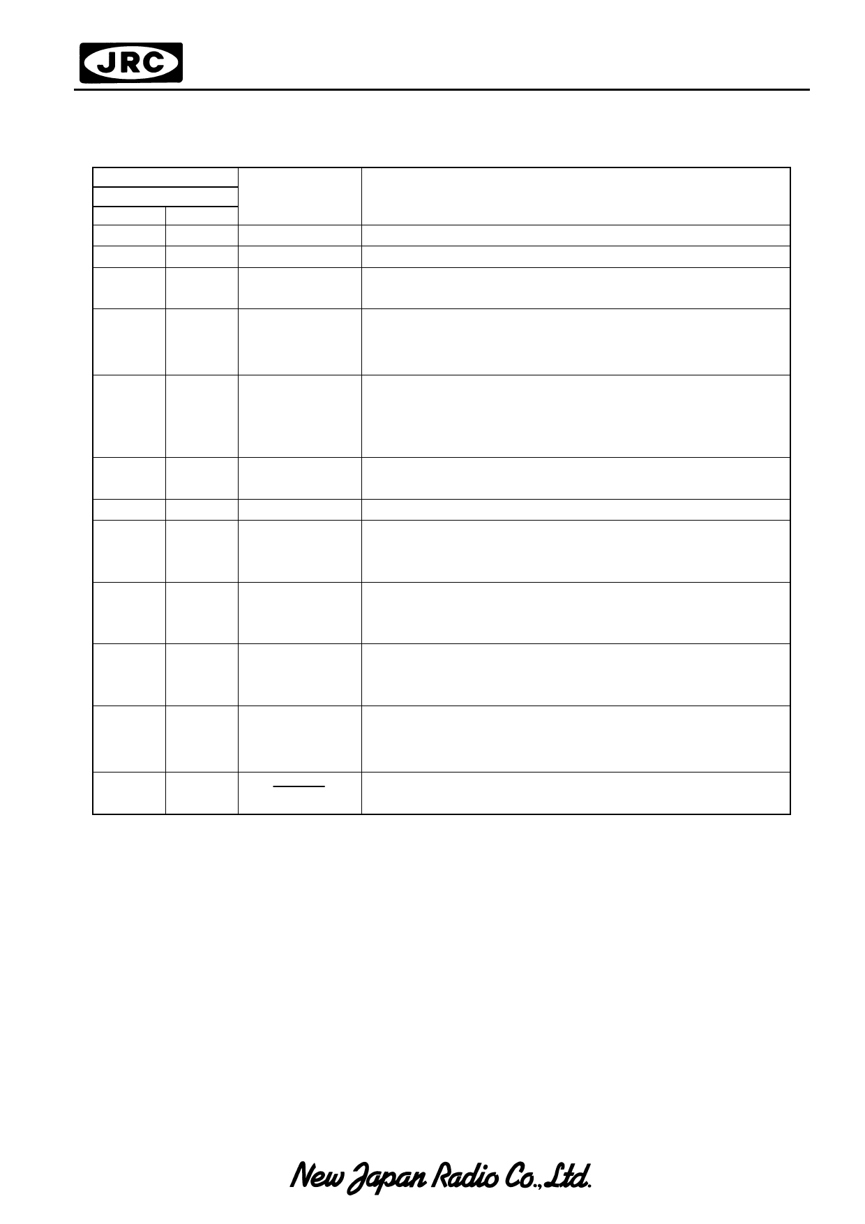
s TERMINAL DESCRIPTION
PAD No.
Pin Configuration
Mode A Mode B
2,3,4
2,3,4
84,85,86 84,85,86
9,8,
9,8,
7,6,5
7,6,5
SYMBOL
VDD
VSS
V2,V3,
V5
82
82
83
83
OSC1
OSC2
11
11
RS
12
12
13
13
22∼19 22∼19
R/W
E
DB7∼DB4
18∼14 18∼14
DB3∼DB0
23∼30
81∼74
81∼74
23∼30
COM1∼COM8
COM9∼COM16
33∼72 72∼33
SEG1∼SEG40
10
10
RESET
FUNCTION
Power Source (+5V)
Power Source ( 0V)
LCD Driving Power Source
Oscillation Frequency Adjust Terminals. Normally Open.
(Oscillation C and R are incorporated, OSC Freq.=270kHz)
For external clock operation, the clock should be input on OSC1.
Register selection signal input
“0” : Instruction Register (Writing)
Busy Flag (Reading)
“1” : Data Register (Writing/Reading)
Read/Write selection signal input
“0” : Write, “1” : Read
Read/Write activation signal input
3-state Data Bus (Upper) to transfer the data between MPU and
NJU6631A
DB7 is also used for the Busy flag reading.
3-state Data Bus (Lower) to transfer the data between MPU and
NJU6631A
These bus are not used in the 4-bit operation.
LCD Common driving signal Terminals
Common driver Location order Select as Shown in Table 4.
Pin configuration mode A : M0=0 / mode B : M0=1.
LCD Segment driving signal Terminals
Segment driver Location order Select as Shown in Table 4.
Pin configuration mode A : M0=0 / mode B : M0=1.
Reset Terminal. When the “L” level input over than 1.2ms to this
terminal the system will be reset. (fOSC=270kHz)
Share Link: 