5108IS データシートの表示(PDF) - Renesas Electronics
部品番号
コンポーネント説明
メーカー
5108IS Datasheet PDF : 13 Pages
| |||
EL5108, EL5308
Absolute Maximum Ratings (TA = +25°C)
Supply Voltage between VS+ and VS- . . . . . . . . . . . . . . . . . . . 13.2V
Pin Voltages . . . . . . . . . . . . . . . . . . . . . . . . . VS- -0.5V to VS+ +0.5V
Maximum Continuous Output Current . . . . . . . . . . . . . . . . . . . 50mA
Maximum Slewrate from VS+ to VS- . . . . . . . . . . . . . . . . . . . . 1V/µs
Thermal Information
Storage Temperature . . . . . . . . . . . . . . . . . . . . . . . .-65°C to +150°C
Ambient Operating Temperature . . . . . . . . . . . . . . . .-40°C to +85°C
Operating Junction Temperature . . . . . . . . . . . . . . . . . . . . . . +125°C
Power Dissipation . . . . . . . . . . . . . . . . . . . . . . . . . . . . . See Curves
Pb-free reflow profile . . . . . . . . . . . . . . . . . . . . . . . . . .see link below
http://www.intersil.com/pbfree/Pb-FreeReflow.asp
CAUTION: Do not operate at or near the maximum ratings listed for extended periods of time. Exposure to such conditions may adversely impact product reliability and
result in failures not covered by warranty.
IMPORTANT NOTE: All parameters having Min/Max specifications are guaranteed. Typical values are for information purposes only. Unless otherwise noted, all tests
are at the specified temperature and are pulsed tests, therefore: TJ = TC = TA
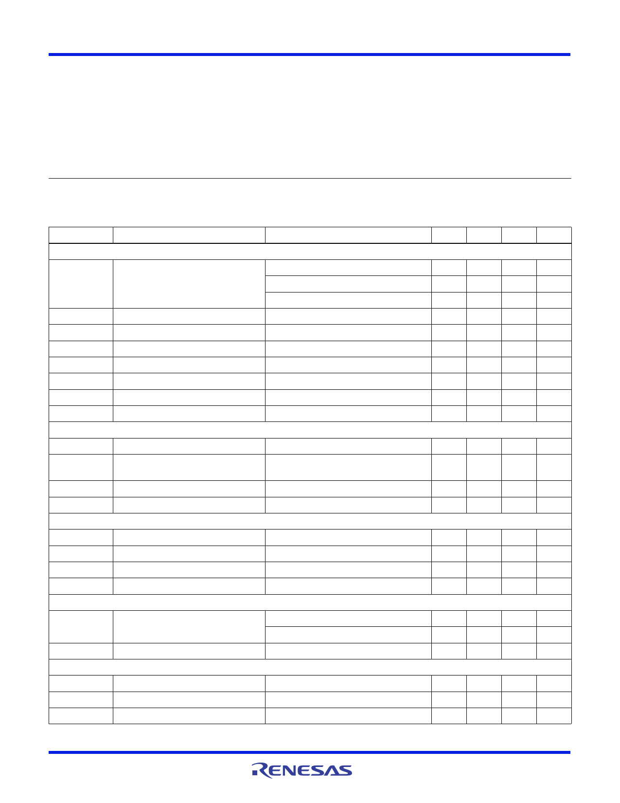
Electrical Specifications VS+ = +5V, VS- = -5V, RL = 150, TA = +25°C Unless Otherwise Specified.
PARAMETER
DESCRIPTION
CONDITIONS
MIN
AC PERFORMANCE
BW
-3dB Bandwidth
BW1
0.1dB Bandwidth
SR
Slew Rate
tS
0.1% Settling Time
eN
Input Voltage Noise
iN
Input Current Noise
dG
Differential Gain Error (Note 1)
dP
Differential Phase Error (Note 1)
DC PERFORMANCE
AV = +1
AV = -1
AV = +2
AV = +2
VO = -2.5V to +2.5V, AV = +2
VOUT = -2.5V to +2.5V, AV = +2
f = 2kHz
AV = +2
AV = +2
3500
VOS
Offset Voltage
-8
TCVOS
Input Offset Voltage Temperature
Coefficient
Measured from TMIN to TMAX
AE
Gain Error
RF, RG
Internal RF and RG
INPUT CHARACTERISTICS
VO = -3V to +3V, RL = 150
CMIR
Common Mode Input Range
±3
+IIN
+ Input Current
RIN
Input Resistance
CIN
Input Capacitance
OUTPUT CHARACTERISTICS
at IN+
VO
Output Voltage Swing
RL = 150 to GND
±3.6
RL = 1k to GND
±3.8
IOUT
Output Current
RL = 10 to GND
100
SUPPLY
ISON
ISOFF
PSRR
Supply Current - Enabled (per amplifier) No load, VIN = 0V
Supply Current - Disabled (per amplifier) No load, VIN = 0V
Power Supply Rejection Ratio
DC, VS = ±4.75V to ±5.25V
3.18
TYP
440
445
450
40
4500
10
2
12
0.01
0.01
+3
5
0.7
325
±3.3
2
0.7
1
±3.8
±4.0
135
3.7
9
75
MAX UNIT
MHz
MHz
MHz
MHz
V/µs
ns
nV/Hz
pA/Hz
%
°
+8
mV
µV/°C
2.5
%
V
8
µA
M
pF
V
V
mA
4.35
mA
25
µA
dB
FN7358 Rev 8.00
August 11, 2015
Page 3 of 13
Share Link: 