5108IS データシートの表示(PDF) - Renesas Electronics
部品番号
コンポーネント説明
メーカー
5108IS Datasheet PDF : 13 Pages
| |||
EL5108, EL5308
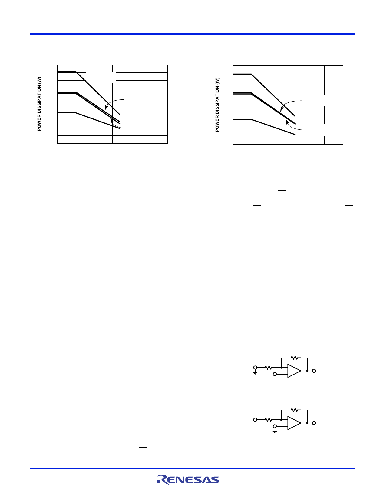
Typical Performance Curves (Continued)
JEDEC JESD51-3 LOW EFFECTIVE THERMAL
CONDUCTIVITY TEST BOARD
1
909mW
0.9
SO16 (0.150”)
0.8
JA=110°C/W
0.7 625mW
0.6 633mW
0.5
SO8
JA=160°C/W
0.4
0.3 391mW
0.2
SOT23-6
JA=256°C/W
0.1
QSOP16
JA=158°C/W
0
0
25
50
75 85 100
125
150
AMBIENT TEMPERATURE (°C)
FIGURE 19. PACKAGE POWER DISSIPATION vs AMBIENT
TEMPERATURE
JEDEC JESD51-7 HIGH EFFECTIVE THERMAL
CONDUCTIVITY TEST BOARD
1.4
1.250W
1.2
1 909mW
SO16 (0.150”)
JA=80°C/W
0.8 893mW
0.6
435mW
0.4
SOT23-6
0.2
JA=230°C/W
0.1
0
0
25
50
SO8
JA=110°C/W
QSOP16
JA=112°C/W
75 85 100 125 150
AMBIENT TEMPERATURE (°C)
FIGURE 20. PACKAGE POWER DISSIPATION vs AMBIENT
TEMPERATURE
Applications Information
Product Description
The EL5108 and EL5308 are fixed gain amplifiers that offer a
wide -3dB bandwidth of 450MHz and a low supply current of
3.5mA per amplifier. They work with supply voltages ranging
from a single 5V to 10V and they are also capable of swinging
to within 1.2V of either supply on the output. These
combinations of high bandwidth, low power, and high slew rate
make the EL5108 and EL5308 the ideal choice for many low-
power/high-bandwidth applications such as portable,
handheld, or battery-powered equipment.
For varying bandwidth and higher gains, consider the EL5166
with 1GHz on a 9mA supply current or the EL5164 with
600MHz on a 3.5mA supply current. Versions include single,
dual, and triple amp packages with 6 Ld SOT-23,
16 Ld QSOP, and 8 Ld SOIC or 16 Ld SOIC outlines.
Power Supply Bypassing and Printed Circuit Board
Layout
As with any high frequency device, good printed circuit board
layout is necessary for optimum performance. Low impedance
ground plane construction is essential. Surface mount
components are recommended, but if leaded components are
used, lead lengths should be as short as possible. The power
supply pins must be well bypassed to reduce the risk of
oscillation. The combination of a 4.7µF tantalum capacitor in
parallel with a 0.01µF capacitor has been shown to work well
when placed at each supply pin.
Disable/Power-Down
The EL5108 and EL5308 amplifiers can be disabled and
placing their outputs in a high impedance state. When
disabled, the amplifier supply current is reduced to <25µA. The
EL5108 and EL5308 are disabled when the CE pin is pulled up
to within 1V of the positive supply. Similarly, the amplifier is
enabled by floating or pulling its CE pin to at least 3V below the
positive supply. For ±5V supply, this means that the amplifier
will be enabled when CE is 2V or less, and disabled when CE
is above 4V. Although the logic levels are not standard TTL,
this choice of logic voltages allow the EL5108 and EL5308 to
be enabled by tying CE to ground, even in 5V single supply
applications. The CE pins can be driven from CMOS outputs.
Gain Setting
The EL5108 and EL5308 are built with internal feedback and
gain resistors. The internal feedback resistors have equal
value; as a result, the amplifier can be configured into gain of
+1, -1, and +2 without any external resistors. Figure 21 shows
the amplifier in gain of +2 configuration. The gain error is ±2%
maximum. Figure 22 shows the amplifier in gain-of-1
configuration. For gain of +1, IN+ and IN- should be connected
together as shown in Figure 23. This configuration avoids the
effects of any parasitic capacitance on the IN- pin. Since the
internal feedback and gain resistors change with temperature
and process, external resistor should not be used to adjust the
gain settings.
325
325
IN-
-
IN+
+
FIGURE 21. AV = +2
325
IN-
GND
325
-
+
FIGURE 22. AV = -1
FN7358 Rev 8.00
August 11, 2015
Page 8 of 13
Share Link: 