IRLS630A データシートの表示(PDF) - Fairchild Semiconductor
部品番号
コンポーネント説明
メーカー
IRLS630A Datasheet PDF : 7 Pages
| |||
IRLS630A
N-CHANNEL
POWER MOSFET
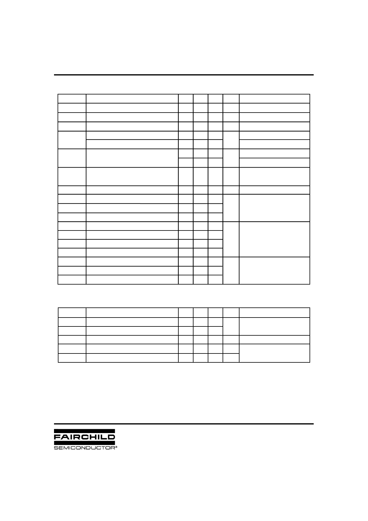
Electrical Characteristics (TC=25℃ unless otherwise specified)
Symbol
BVDSS
ΔBV/ΔTJ
VGS(th)
IGSS
IDSS
RDS(on)
gfs
Ciss
Coss
Crss
td(on)
tr
td(off)
tf
Qg
Qgs
Qgd
Characteristic
Min. Typ. Max. Units
Test Condition
Drain-Source Breakdown Voltage
Breakdown Voltage Temp. Coeff.
Gate Threshold Voltage
Gate-Source Leakage , Forward
Gate-Source Leakage , Reverse
Drain-to-Source Leakage Current
200 -- -- V
-- 0.18 -- V/℃
1.0 -- 2.0 V
-- -- 100 nA
-- -- -100
-- -- 10
-- -- 100 μA
VGS=0V,ID=250μA
ID=250μA See Fig 7
VDS=VGS, ID=250μA
VGS=20V
VGS=-20V
VDS=200V
VDS=160V,TC=125℃
Static Drain-Source
On-State Resistance
-- -- 0.4 Ω VGS=5V,ID=3.25A ④
Forward Transconductance
Input Capacitance
Output Capacitance
Reverse Transfer Capacitance
-- 4.5 -- S VDS=40V,ID=3.25A ④
-- 580 755
-- 90 115 pF VGS=0V,VDS=25V,f =1MHz
See Fig 5
-- 44 55
Turn-On Delay Time
Rise Time
Turn-Off Delay Time
Fall Time
-- 8 25
--
--
6
30
20
70
VDD=100V,ID=9A,
ns RG=6Ω
See Fig 13 ④ ⑤
-- 9 30
Total Gate Charge
Gate-Source Charge
Gate-Drain("Miller") Charge
-- 18.6 27
-- 3.5 --
-- 8.3 --
VDS=160V,VGS=5V,
nC ID=9A
See Fig 6 & Fig 12 ④ ⑤
Source-Drain Diode Ratings and Characteristics
Symbol
IS
ISM
VSD
trr
Qrr
Characteristic
Continuous Source Current
Pulsed-Source Current
Diode Forward Voltage
Reverse Recovery Time
Reverse Recovery Charge
Min. Typ. Max. Units
Test Condition
--
① --
-- 9
-- 32
Integral reverse pn-diode
A
in the MOSFET
④ -- -- 1.5 V TJ=25℃,IS=6.5A,VGS=0V
-- 158 -- ns TJ=25℃,IF=9A
-- 0.78 -- μC diF/dt=100A/μs
④
Notes ;
① Repetitive Rating : Pulse Width Limited by Maximum Junction Temperature
② L=2mH, IAS=6.5A, VDD=50V, RG=27Ω, Starting TJ =25℃
③ ISD≤9A, di/dt≤220A/μs, VDD≤BVDSS , Starting TJ =25℃
④ Pulse Test : Pulse Width = 250μs, Duty Cycle ≤ 2%
⑤ Essentially Independent of Operating Temperature
Share Link: 