TDA8034AT データシートの表示(PDF) - NXP Semiconductors.
部品番号
コンポーネント説明
メーカー
TDA8034AT Datasheet PDF : 30 Pages
| |||
NXP Semiconductors
TDA8034T; TDA8034AT
Smart card interface
8.3 Clock circuits
The clock signal from pin CLK to the card is either supplied by an external clock signal
connected to pin XTAL1 or generated using a crystal connected between pins XTAL1 and
XTAL2. The TDA8034T/TDA8034AT automatically detects if an external clock is
connected to XTAL1, eliminating the need for a separate pin to select the clock source.
Automatic clock source detection is performed on each activation command (falling edge
of the signal on pin CMDVCCN). The presence of an external clock on pin XTAL1 is
checked during a time window defined by the internal oscillator. If a clock is detected, the
internal crystal oscillator is stopped. If a clock is not detected, the internal crystal oscillator
is started. When an external clock is used, it is mandatory that the clock is applied to pin
XTAL1 before the falling edge of the signal on pin CMDVCCN.
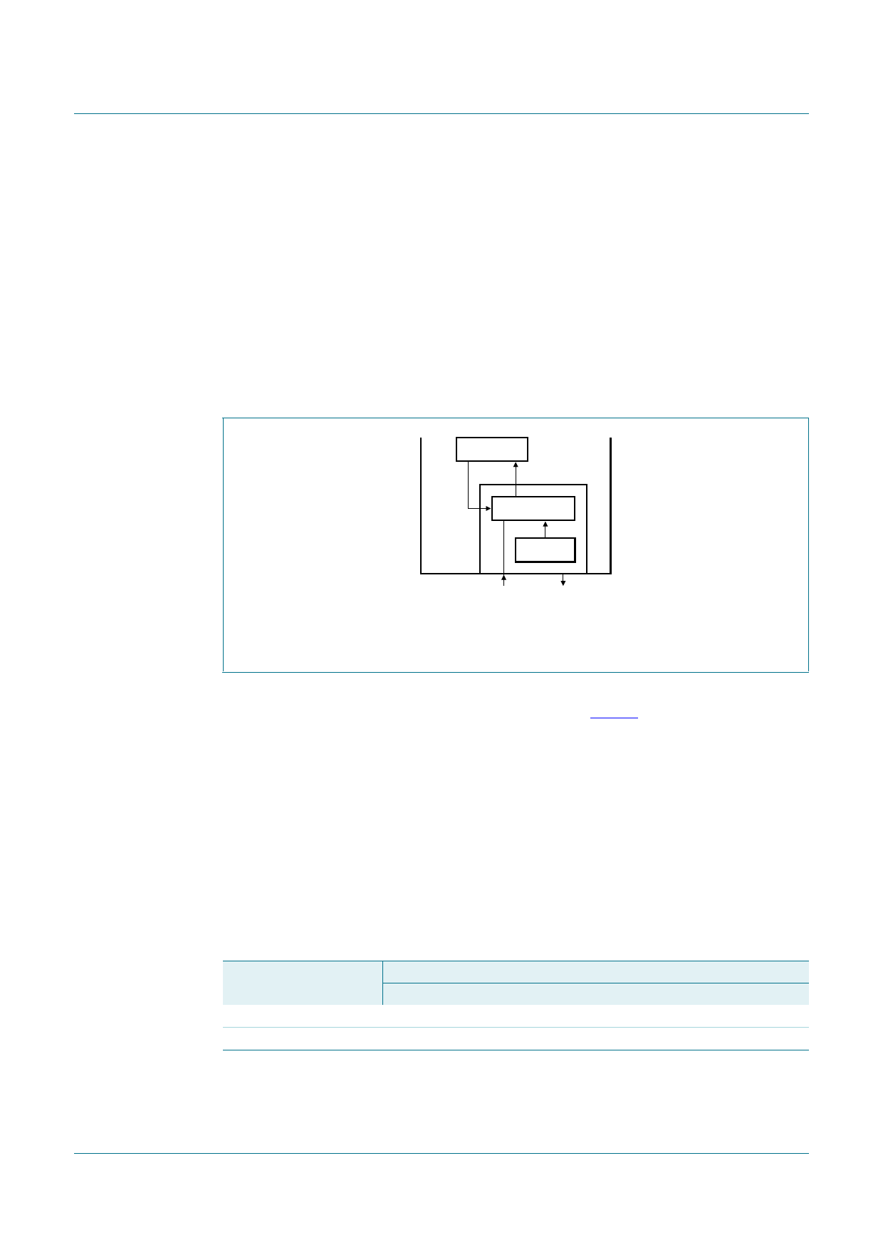
DIGITAL
enclkin
clkxtal
MULTIPLEXER
CRYSTAL
XTAL1
XTAL2
001aak992
enclkin and clkxtal are internal signal names.
Fig 5. Basic layout for using an external clock
The clock frequency is selected using pin CLKDIV1 to be either 1⁄2 fxtal or 1⁄4 fxtal on
TDA8034T or fxtal or 1⁄2 fxtal on TDA8034AT as shown in Table 4.
The frequency change is synchronous and as such during transition, no pulse is shorter
than 45 % of the smallest period. In addition, only the first and last clock pulse around the
change has the correct width. When dynamically changing the frequency, the modification
is only effective after 10 clock periods on pin XTAL1.
The duty cycle of fxtal on pin CLK should be between 45 % and 55 %. If an external clock
is connected to pin XTAL1, its duty cycle must be between 48 % and 52 %.
When the frequency of the clock signal on pin CLK is either 1⁄2 fxtal or 1⁄4 fxtal on TDA8034T
or fxtal or 1⁄2 fxtal on TDA8034AT, the frequency dividers guarantee a duty cycle between
45 % and 55 %.
Table 4. Clock configuration
Pin CLKDIV1 level
Pin CLK level
TDA8034T
HIGH
LOW
1⁄2 fxtal
1⁄4 fxtal
TDA8034AT
1⁄2 fxtal
fxtal
TDA8034T_TDA8034AT
Product data sheet
All information provided in this document is subject to legal disclaimers.
Rev. 3.1 — 13 December 2012
© NXP B.V. 2012. All rights reserved.
7 of 30
Share Link: 