Q62702-G0080 データシートの表示(PDF) - Infineon Technologies
部品番号
コンポーネント説明
メーカー
Q62702-G0080 Datasheet PDF : 24 Pages
| |||
GaAs Components
CGY 196
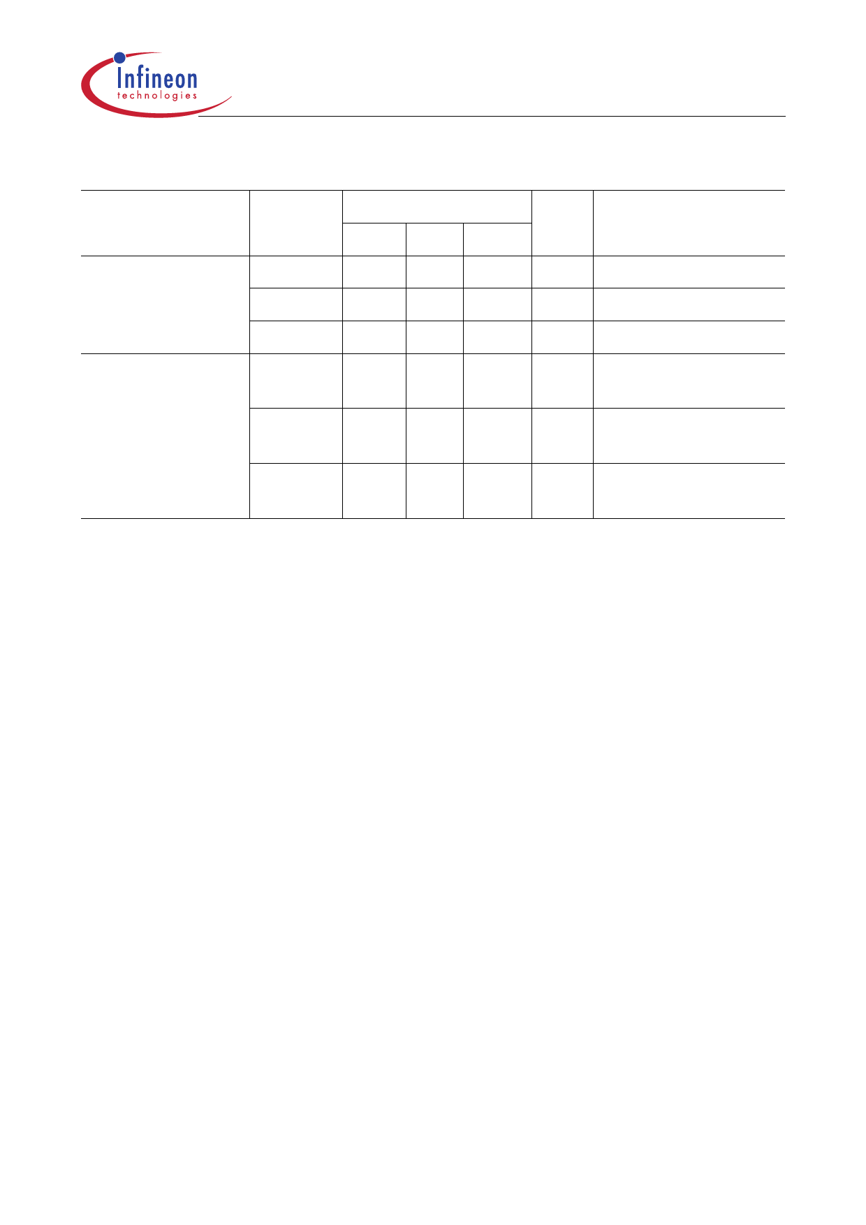
DC Characteristics
Characteristics Symbol
Drain current
stage 1 - 3
Transconductance
stage 1 - 3
IDSS1
IDSS2
IDSS3
GFS1
GFS2
GFS3
Limit Values
min. typ. max.
30 45 75
45 65 110
230 340 515
50 90 130
80 130 170
150 220 300
Unit
mA
mA
mA
mS
mS
mS
Test Conditions
VD1 = 3 V
VD2 = 3 V
VD3 = 3 V
VD = 3 V,
ID = 50 mA
VD = 3 V,
ID = 300 mA
VD = 3 V,
ID = 300 mA
Determination of Permissible Total Power Dissipation for Continuous and Pulse
Operation
The dissipated power is the power which remains in the chip and heats the device. It
does not contain RF signals which are coupled out consistently.
a) Continuous Wave/DC Operation
For the determination of the permissible total power dissipation Ptot-DC from the diagram
below it is necessary to obtain the temperature of the soldering point TS first. There are
two cases:
• When RthSA (soldering point to ambient) is not known: Measure TS with a temperature
sensor at the leads were the heat is transferred from the device to the board
(normally at the widest source or ground lead for GaAs). Use a small sensor of low
heat transport, for example a thermoelement (< 1 mm) with thin wires or a
temperature indicating paper while the device is operating.
• When RthSA is already known: TS = PDiss × RthSA + TA
Data Sheet
3
2001-01-01
Share Link: 