CGY196 データシートの表示(PDF) - Siemens AG
部品番号
コンポーネント説明
メーカー
CGY196 Datasheet PDF : 15 Pages
| |||
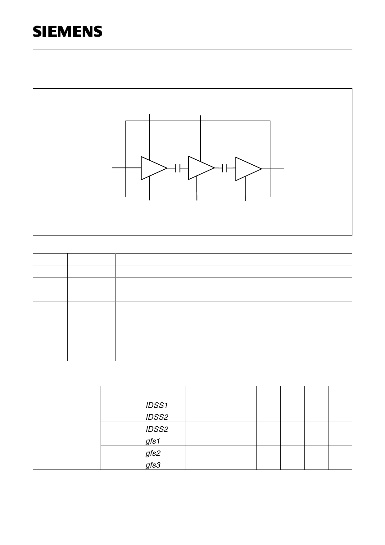
Functional Block Diagram
VD1
VD2
CGY 196
RFin/Vg
GND
GND
GND
RFout/Vd3
Pin #
1
2
3
4
5
6
7
8
Name Configuration
RFin/Vg RF input power + Gate voltage [0V internal]
GND RF and DC ground
VD2 Pos. drain voltage of the 2nd stage
n.c. not connected
n.c. not connected
RFout/VD3 RF output power / Pos. drain voltage of the 3rd stage
GND RF and DC ground
VD1 Pos. drain voltage of the 1st stage
DC characteristics
Characteristics
Drain current
stage 1
stage 2
stage 3
Transconductance stage 1
stage 2
stage 3
Symbol
IDSS1
IDSS2
IDSS2
gfs1
gfs2
gfs3
Conditions
min typ max Unit
VD1=3V
45
mA
VD2=3V
65
mA
VD2=3V
340
mA
VD=3V, ID=50mA
110
mS
VD=3V, ID=300mA
650
mS
VD=3V, ID=300mA
650
mS
Siemens Aktiengesellschaft
2
Semiconductor Group
2
16.6.1998
HL HF19P9E8-G11a-A0s1
Share Link: 