CGY196 データシートの表示(PDF) - Siemens AG
部品番号
コンポーネント説明
メーカー
CGY196 Datasheet PDF : 15 Pages
| |||
CGY 196
Electrical characteristics [ 3.0V DECT-Application: PCB-Layout see page 9]
(TA = 25°C , f=1.89 GHz, ZS=ZL=50 Ohm, unless otherwise specified)
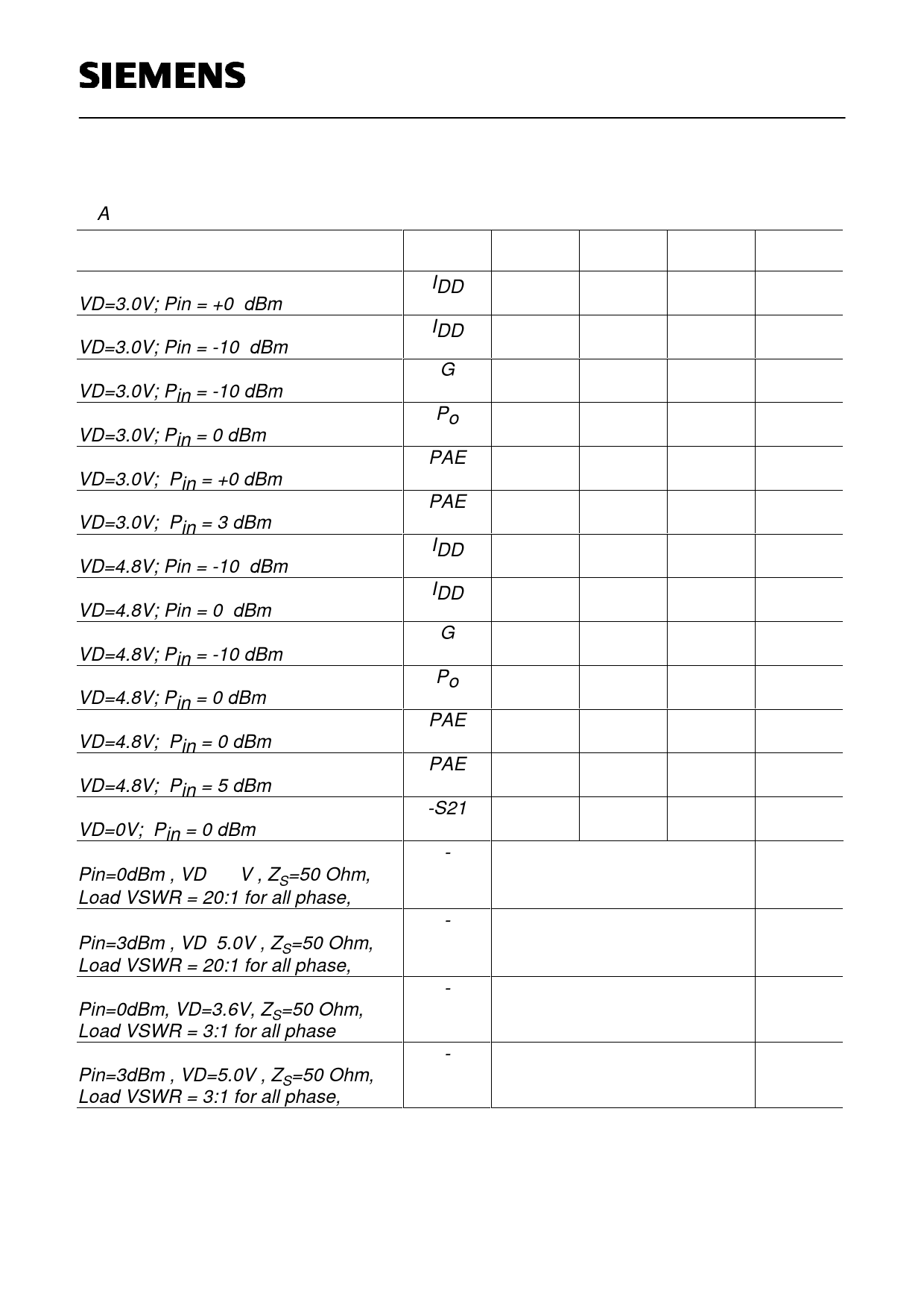
Characteristics
Symbol min
typ
max
Unit
Supply current
VD=3.0V; Pin = +0 dBm
Supply current
VD=3.0V; Pin = -10 dBm
Gain
VD=3.0V; Pin = -10 dBm
Output Power
VD=3.0V; Pin = 0 dBm
Overall Power added Efficiency
VD=3.0V; Pin = +0 dBm
Overall Power added Efficiency
VD=3.0V; Pin = 3 dBm
Supply current
VD=4.8V; Pin = -10 dBm
Supply current
VD=4.8V; Pin = 0 dBm
Gain
VD=4.8V; Pin = -10 dBm
Output Power
VD=4.8V; Pin = 0 dBm
Overall Power added Efficiency
VD=4.8V; Pin = 0 dBm
Overall Power added Efficiency
VD=4.8V; Pin = 5 dBm
Off Isolation
VD=0V; Pin = 0 dBm
Load mismatch
Pin=0dBm , VD≤3.6V , ZS=50 Ohm,
Load VSWR = 20:1 for all phase,
Load mismatch
Pin=3dBm , VD≤5.0V , ZS=50 Ohm,
Load VSWR = 20:1 for all phase,
Stability
Pin=0dBm, VD=3.6V, ZS=50 Ohm,
Load VSWR = 3:1 for all phase
Stability
Pin=3dBm , VD=5.0V , ZS=50 Ohm,
Load VSWR = 3:1 for all phase,
IDD
IDD
G
Po
PAE
PAE
IDD
IDD
G
Po
PAE
PAE
-S21
-
-
-
-
-
300
-
-
450
-
32
26.0
45
-
50
-
-
450
-
-
370
-
-
32
-
29
45
-
50
-
40
No module damage
for 10 sec.
No module damage
for 10 sec.
All spurious output
more than 70 dB below
desired signal level
All spurious output
more than 70 dB below
desired signal level
mA
mA
dB
dBm
%
%
mA
mA
dB
dBm
%
%
dB
-
-
-
-
Siemens Aktiengesellschaft
6
Semiconductor Group
6
16.6.1998
HL HF19P9E8-G11a-A0s1
Share Link: 