FAN5631 データシートの表示(PDF) - Fairchild Semiconductor
部品番号
コンポーネント説明
メーカー
FAN5631 Datasheet PDF : 14 Pages
| |||
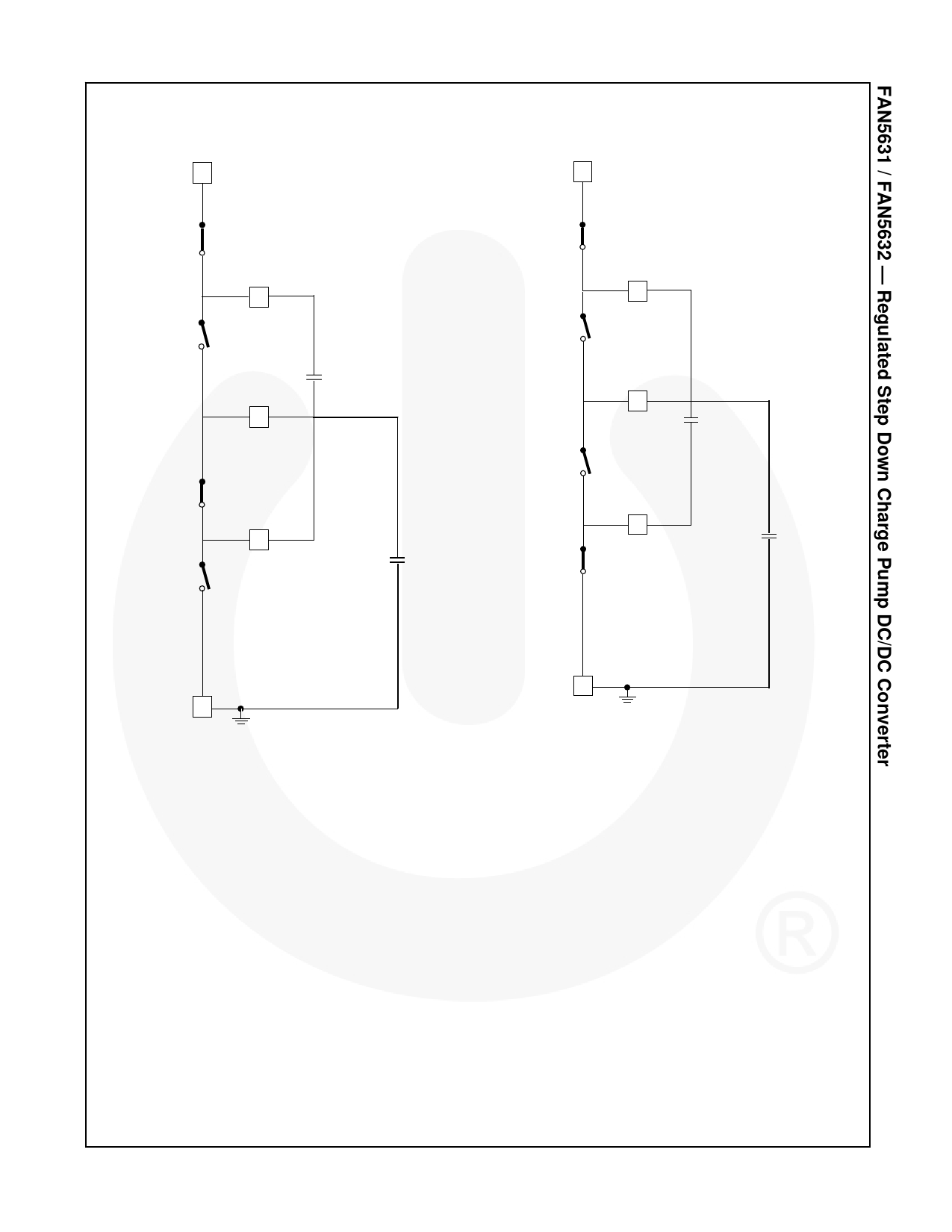
Switch Configuration
VIN
S1
C+
S2
C
B
VOUT
S3
C-
S4
C
OUT
VIN
S1
C+
S2
VOUT
C
B
S3
C-
S4
C
OUT
GND
2:1 configuration
Switches in charging phase
Reverse all switches for pumping phase
Figure 15. 2:1 Configuration
GND
1:1 configuration
Switch 3 is always off
Switch 4 is always on
Switches 1 and 2 are in phase 1
Reverse position of switches 1&2 for phase 2
Figure 16. 1:1 Configuration
Shutdown, UVLO, Short-Circuit,
Current-Limit and Thermal Shutdown
The device has an active-low shutdown pin to decrease
supply current to less than 1μA. In shutdown mode, the
supply is disconnected from the output. UVLO triggers
when supply voltage drops below 2V. When the output
voltage is lower than 150mV, a short-circuit protection is
triggered. In this mode, 15 out of 16 pulses during the
switching are skipped and the supply current is limited.
Thermal shutdown triggers at 150ºC.
Efficiency Optimizer (FAN5632)
In the FAN5632, VSEL can be tied to ground to enable
the efficiency optimizer feature. To achieve an
optimized efficiency, the switch mode configuration
transition point is shifted from a 2:1 to a 1:1 mode until
the output voltage falls to 20% of its nominal value. For
example, when the nominal output voltage is 1.5V, the
output voltage is allowed to drop to 1.2V. This maintains
a peak efficiency of 85% for the input voltage range of
2.9V to 3.5V. For normal operation, tie VSEL high.
© 2006 Fairchild Semiconductor Corporation
FAN5631/FAN5632 Rev. 1.0.2
9
www.fairchildsemi.com
Share Link: 