FAN8060 データシートの表示(PDF) - ON Semiconductor
部品番号
コンポーネント説明
メーカー
FAN8060 Datasheet PDF : 14 Pages
| |||
The system pole is calculated by the equation:
fP1
=
2π
1
⋅ COUT
⋅ RL
(7)
The system zero is due to the output capacitor and its
ESR. System zero is calculated by the equation:
fz1
=
2π
1
⋅ COUT
⋅ ESR
(8)
The output characteristics of the error (Gm) amplifier
are controlled by a series capacitor and resistor
network connected at the COMP pin to GND.
The pole is calculated by the following equation:
fp2
=
2π
GEA
⋅ CC ⋅ AVEA
(9)
where:
GEA = Error Amplifier Transconductance (1000 µA/V);
and
CC = compensation capacitor.
Zero is due to the compensation capacitor (CC) and
resistor (RC) calculated by the following equation:
fz2
=
2π
1
⋅ CC
⋅ RC
(10)
where RC is compensation resistor.
The system crossover frequency (fC), where the control
loop has unity gain, is recommended to be set at 1/10th
of switching frequency. Generally, higher fC means
faster response to load transients, but can result in
instability if not properly compensated.
The first step in compensation design is choosing the
compensation resistor (RC) to set the crossover
frequency by the following equation:
RC
=
2π ⋅ COUT ⋅ fC ⋅VOUT
GCS ⋅ GEA ⋅VFB
(11)
where VFB is reference voltage.
The next step is choosing the compensation capacitor
(CC) to achieve the desired phase margin. For
applications with typical inductor values, setting the
compensation zero, fZ2, to below one fourth of the
crossover frequency provides sufficient phase margin.
Determine the (CC) value by the following equation:
CC
=
π
2
⋅ RC
⋅ fC
(12)
Then determine if the second compensation capacitor
(CA) is required. It is required if the ESR zero of the
output capacitor is located at less than half of the
switching frequency.
1
< fS
2π ⋅ COUT ⋅ ESR 2
(13)
If required, add the second compensation capacitor
(CA) to set the pole fP3 at the location of the ESR zero.
Determine (CA) value by the equation:
CA
=
COUT ⋅ ESR
RC
(14)
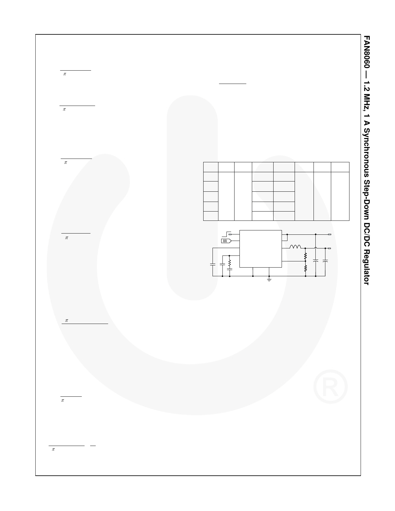
Design Example
Table 2 provides component values for delivering
various output voltages with loads up to 1 A with VIN at
5 V (±10% tolerance).
Table 2. Recommended Feedback and
Compensation Values (VIN=5 V)
VO C4 L1
R2
R3
R1 C5 C2
1.2 V
Short Open
1.5 V
2.55 kΩ 10.2 kΩ
1.8 V 10 µF 3.3 µH 5.9 kΩ 11.8 kΩ 4.7 kΩ 1.5 nF 150 pF
2.5 V
16.2 kΩ 15 kΩ
3.3 V
18.7 kΩ 10.7 kΩ
HI
LO
EN
PVIN
SYNC
AVIN
SS
FAN8060 SW
C1 C2
10nF 150pF
COMP
R1
4.7k
AGND
C5
1.5nF
FB
PGND
INPUT
2.5 to 5.5V
L1
3.3µH
R2
16.2k
OUTPUT
2.5V/1A
C3 C4
R3 10µF 10µF
15k
Figure 15. Recommended Schematic (5 VIN to
2.5 VO)
© 2013 Fairchild Semiconductor Corporation
FAN8060 • Rev. 1.0.1
10
www.fairchildsemi.com
Share Link: 