AD1990 データシートの表示(PDF) - Analog Devices
部品番号
コンポーネント説明
メーカー
AD1990 Datasheet PDF : 16 Pages
| |||
AD1990
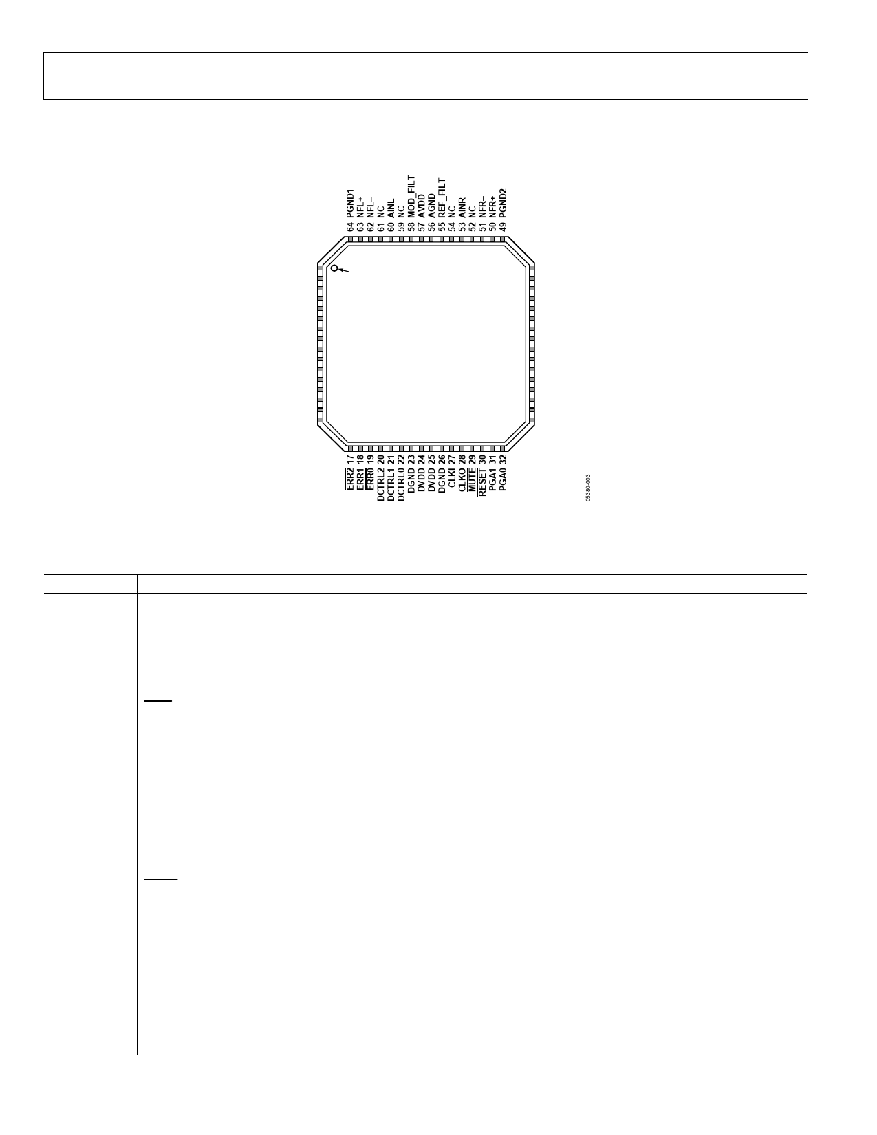
PIN CONFIGURATION AND FUNCTION DESCRIPTIONS
PGND1 1
PGND1 2
PGND1 3
OUTL+ 4
OUTL+ 5
OUTL+ 6
PVDD1 7
PVDD1 8
PVDD1 9
PVDD1 10
OUTL– 11
OUTL– 12
OUTL– 13
PGND1 14
PGND1 15
PGND1 16
PIN 1
INDICATOR
AD1990
TOP VIEW
(Not to Scale)
NC = NO CONNECT
48 PGND2
47 PGND2
46 PGND2
45 OUTR+
44 OUTR+
43 OUTR+
42 PVDD2
41 PVDD2
40 PVDD2
39 PVDD2
38 OUTR–
37 OUTR–
36 OUTR–
35 PGND2
34 PGND2
33 PGND2
Figure 3. Pin Configuration
Table 9. Pin Function Descriptions
Pin No.
Mnemonic In/Out
1, 2, 3, 64
PGND1
4, 5, 6
OUTL+
O
7, 8, 9, 10
PVDD1
11, 12, 13
OUTL−
O
14, 15, 16
PGND1
17
ERR2
O
18
ERR1
O
19
ERR0
O
20
DCTRL2
I/O
21
DCTRL1
I
22
DCTRL0
I
23, 26
DGND
24, 25
DVDD
27
CLKI
I
28
CLKO
O
29
MUTE
I
30
RESET
I
31
PGA1
I
32
PGA0
I
33, 34, 35
PGND2
36, 37, 38
OUTR−
O
39, 40, 41, 42 PVDD2
43, 44, 45
OUTR+
O
46, 47, 48, 49 PGND2
50
NFR+
I
51
NFR−
I
Description
Negative Power Supply. Used for the A2 and B2 high power transistors.
Output of Transistor Pair A1 and A2.
Positive Power Supply. Used for the A1 and B1 high power transistors.
Output of Transistor Pair B1 and B2.
Negative Power Supply. Used for the A2 and B2 high power transistors.
Active Low Thermal Shutdown Error Output.
Active Low Thermal Warning Error Output.
Active Low Overcurrent Error Output.
Nonoverlap Time Setting MSB.
Nonoverlap Time Setting.
Nonoverlap Time Setting LSB.
Negative Power Supply for Low Power Digital Circuitry.
Positive Power Supply for Low Power Digital Circuitry.
Clock Input for 256 × fS Audio Modulator Clock.
Inverted Version of CLKI for Use with an External XTAL Oscillator.
Active Low Mute Input.
Active Low Reset Input.
PGA Gain Control MSB.
PGA Gain Control LSB.
Negative Power Supply for High Power Transistors C2 and D2.
Output of Transistor Pair D1 and D2.
Positive Power Supply for High Power Transistors C1 and D1.
Output of Transistor Pair C1 and C2.
Negative Power Supply for High Power Transistors C2 and D2.
Right Channel Negative Feedback—Noninverting Input.
Right Channel Negative Feedback—Inverting Input.
Rev. 0 | Page 6 of 16
Share Link: 