CGY181 データシートの表示(PDF) - Siemens AG
部品番号
コンポーネント説明
メーカー
CGY181 Datasheet PDF : 14 Pages
| |||
GaAs MMIC
CGY 181
________________________________________________________________________________________________________
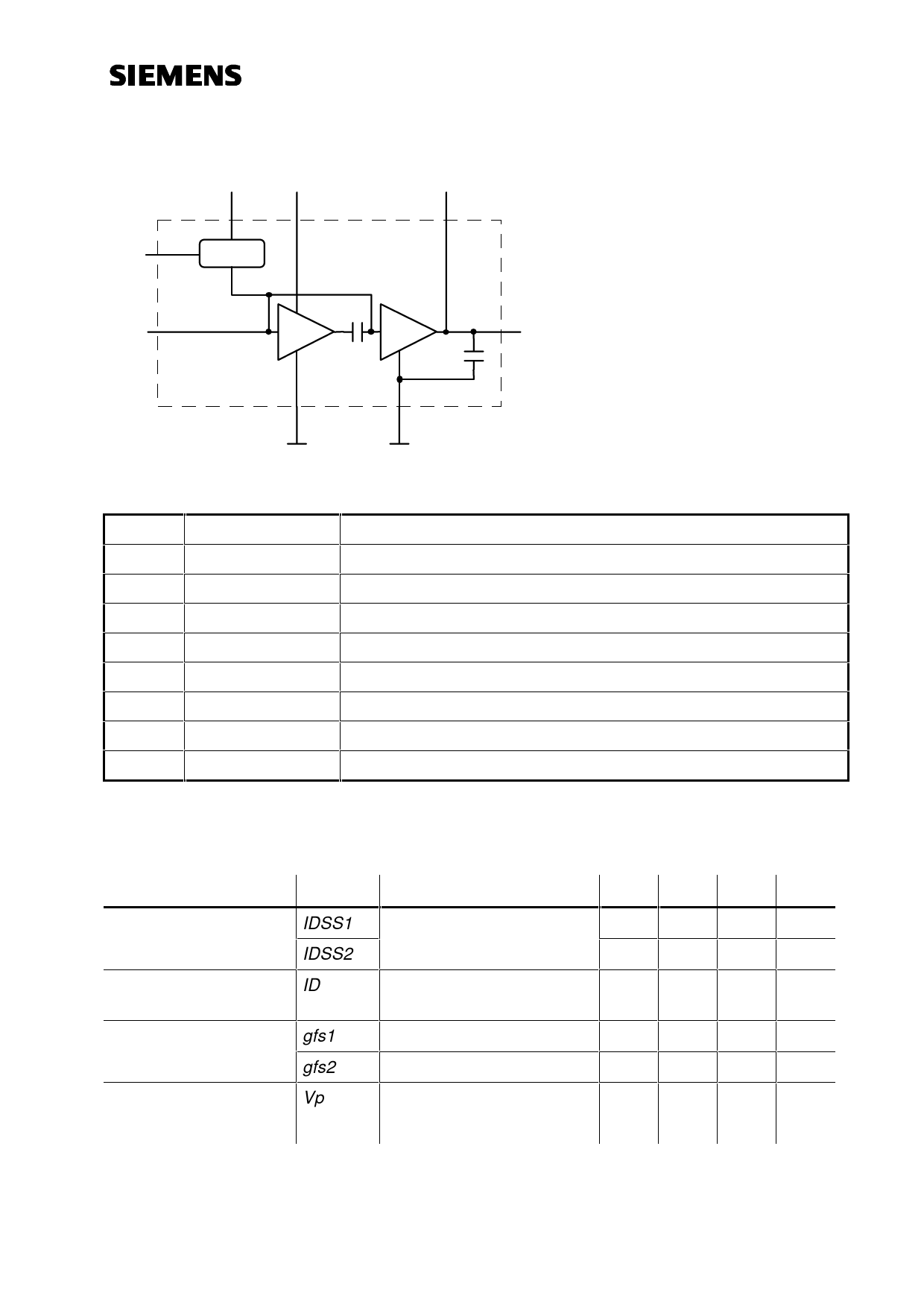
Functional block diagramm:
VG (1)
VD1 (7)
VTR (2)
Control
Circuit
Pin (8)
GND1 (6,9)
connected (shut off mode).
VD2 (11)
Short description of CGY181
operation:
GND2
(3, 4, 5, 10)
Pout (11)
A negative voltage between -4V to -6V
(stabilization not necessary) has to be
connected to the VG-pin, a positive
supply voltage has to be applied to the
VD-pins.
The VTR-pin has to switched to 0V
(GND) during transmit operation. The
MMIC CGY181 is self-biased, the
operating current is adjusted by the
internal control circuit.
In receive mode the VTR-pin is not
Pin #
1
2
3,4,5,10
6,9
7
8
11
12
VG
VTR
GND 2
GND 1
VD1
RFin
VD2,RFout
-
Configuration
Negative voltage at control circuit (-4V...-8V)
Control voltage for transmit mode (0V) or receive mode (open)
RF and DC ground of the 2nd stage
RF and DC ground of the 1st stage
Positive drain voltage of the 1st stage
RF input power
Positive drain voltage of the 2nd stage, RF output power
not connected
DC characteristics
Characteristics
Symbol Conditions
min typ max Unit
Drain current stage 1 IDSS1 VD=3V, VG=0V, VTR n.c. 0.6 0.9 1.2 A
stage 2 IDSS2
2.4 3.5 4.8 A
Drain current with
ID
VD=3V, VG=-4V, VTR=0V
1.0
A
active current control
Transconductance
gfs1
VD=3V, ID=350mA
0.28 0.32 -
S
(stage 1 and 2)
gfs2
VD=3V, ID=700mA
1.1 1.3 -
S
Pinch off voltage
Vp
VD=3V, ID<500µA
-3.8 -2.8 -1.8 V
(all stages)
Siemens Aktiengesellschaft
pg. 2/14
01.02.96
HL EH PD 21
Share Link: 