AM24LC02 データシートの表示(PDF) - Anachip Corporation
部品番号
コンポーネント説明
メーカー
AM24LC02 Datasheet PDF : 12 Pages
| |||
2-Wire Serial 2K-bits (256 x 8) CMOS Electrically Erasable PROM
ATC
AM24LC02
Pin Descriptions
Serial Clcok (SCL)
The SCL input is used to clock all data into and out
of the device.
SerialL Data (SDA)
SDA is a bidirection pin used to transfer data or
security bit into and out of the device. It is an open
drain output and may be wire-ORed with any
number of open drain or open collector outputs.
Thus, the SDA bus requires a pull-up resistor to Vcc
(typical 4.7KΩ for 100KHz, 1KΩ for 400KHz).
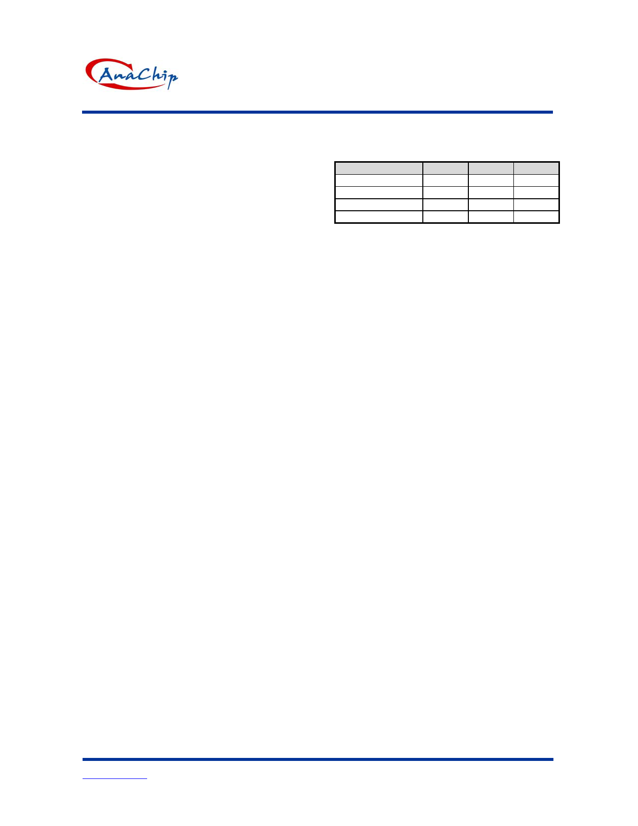
Device Address Inputs (A0, A1, A2)
The following table (Table A) shows the active pins
across the AM24LCXX device family.
TABLE A
Device
A0
A1
A2
AM24LC02
ADR ADR ADR
AM24LC04
XP
ADR ADR
AM24LC08
XP
XP
ADR
AM24LC16
XP
XP
XP
ADR indicates the device address pin.
XP indicates that device address pin does not care
but refers to an internal PAGE BLOCK memory
segment.
Write Protection (WP)
If WP is connected to Vcc, PROGRAM operation
onto the whole memory will not be executed. READ
operations are possible. If WP is connected to Vss,
normal memory operation is enabled, READ/WRITE
over the entire memory is possible.
Functional Description
Applications
ATC’s electrically erasable programmable read only
memories (EEPROMs) offer valuable security
features including write protect function, two write
modes, three read modes, and a wide variety of
memory size. Typical applications for the I2C bus
and
AM24LCXX
memories
include
SANs(small-area-networks), stereos, televisions,
automobiles and other scaled-down systems that do
not require tremendous speeds but instead cost
efficiency and design simplicity.
Endurance And Data Retention
The AM24LC02 is designed for applications
requiring up to 1KK programming cycles (BYTE
WRITE and PAGE WRITE). It provides 40 years of
secure data retention without power.
Device Operation
The AM24LC02 device supports a bidirectional bus
oriented protocol. The protocol defines any device
that sends data onto the bus as a transmitter and
the receiving device as the receiver. The device
controlling the transfer is the master and the device
being controlled is the slave. The master will always
initiate data transfers and provide the clock for both
transmit and receive operations. Therefore, the
AM24LC02 is considered a slave in all applications.
Clock and Data Conventions
Data states on the SDA line can be changed only
during SCL LOW. SDA state changes during SCL
HIGH are reserved for indicating start and stop
conditions. (Shown in Figures 1 and 2)
Start Condition
A HIGH to LOW transition of the SDA line while the
clock (SCL) is HIGH determines a START condition.
All commands must be preceded with a START
condition. (Shown in Figure 2)
Stop Condition
A LOW to HIGH transition of the SDA line while the
clock (SCL) is HIGH determines a STOP condition.
All operations must be ended with a STOP condition.
(Shown in Figure 2)
Anachip Corp.
www.anachip.com.tw
Rev. A1 Oct 20, 2003
4/12
Share Link: 