MCM32515 データシートの表示(PDF) - Motorola => Freescale
部品番号
コンポーネント説明
メーカー
MCM32515 Datasheet PDF : 8 Pages
| |||
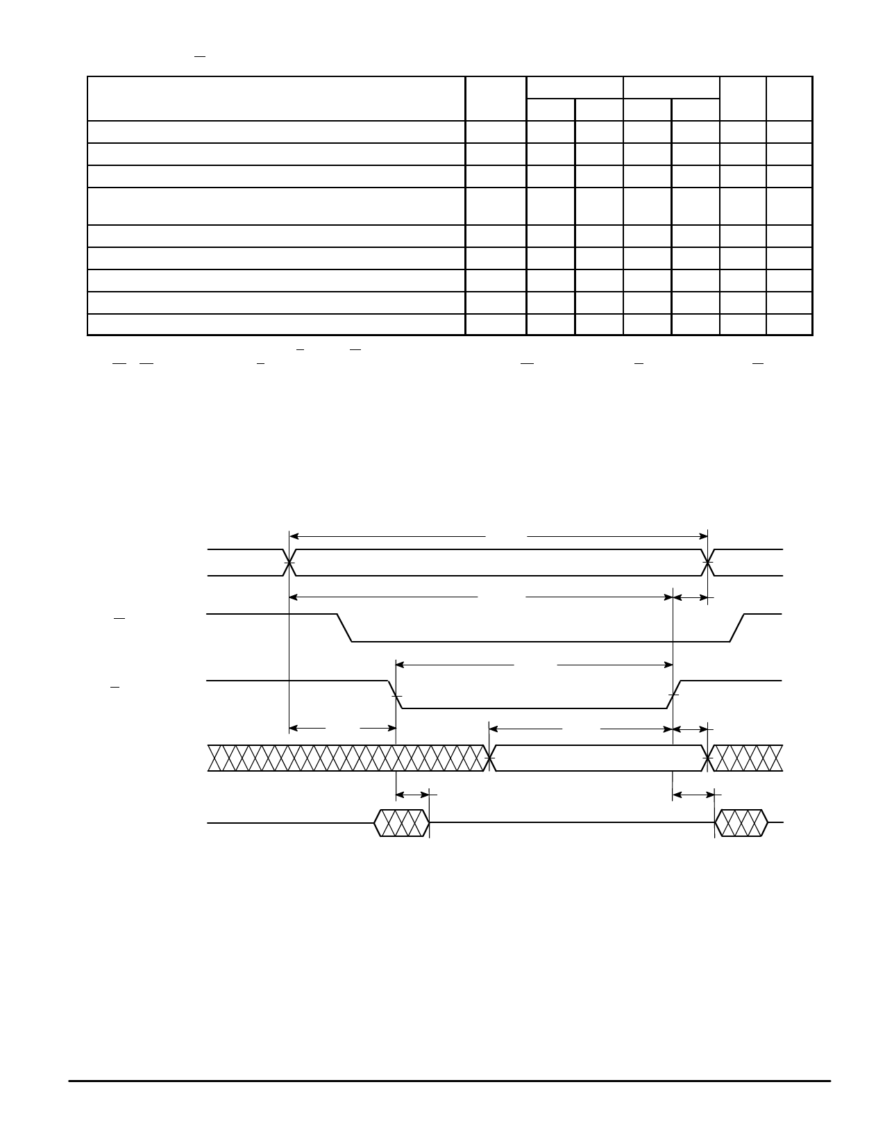
WRITE CYCLE 1 (W Controlled, See Notes 1 and 2)
MCM32515–20 MCM32515–25
Parameter
Symbol Min Max Min Max Unit Notes
Write Cycle Time
Address Setup Time
Address Valid to End of Write
Write Pulse Width
tAVAV
20
—
25
—
ns
3
tAVWL
0
—
0
—
ns
tAVWH
15
—
17
—
ns
tWLWH, 15
—
17
—
ns
tWLEH
Data Valid to End of Write
tDVWH 10
—
10
—
ns
Data Hold Time
tWHDX
0
—
0
—
ns
Write Low to Data High–Z
tWLQZ
0
9
0
10
ns 4,5,6
Write High to Output Active
tWHQX
5
—
5
—
ns 4,5,6
Write Recovery Time
tWHAX
0
—
0
—
ns
NOTES:
1. A write occurs during the overlap of E low and W low.
2. E1 – E4 are represented by E in these timing specifications, any combination of Exs may be asserted. G is a don‘t care when W is low.
3. All write cycle timing is referenced from the last valid address to the first transitioning address.
4. Transition is measured ± 500 mV from steady–state voltage with load of Figure 1b.
5. This parameter is sampled and not 100% tested.
6. At any given voltage and temperature, tWLQZ max is less than tWHQX min both for a given device and from device to device.
A (ADDRESS)
Ex (BYTE ENABLE)
W (WRITE ENABLE)
D (DATA IN)
Q (DATA OUT)
WRITE CYCLE 1
tAVAV
tAVWH
tAVWL
HIGH–Z
tWLWH
tWLQZ
tDVWH
DATA VALID
HIGH–Z
tWHAX
tWHDX
tWHQX
MCM32515
6
MOTOROLA FAST SRAM
Share Link: 