CAT25C32P-TE13 データシートの表示(PDF) - Catalyst Semiconductor => Onsemi
部品番号
コンポーネント説明
メーカー
CAT25C32P-TE13 Datasheet PDF : 11 Pages
| |||
CAT25C32/64
READ Sequence
The part is selected by pulling CS low. The 8-bit read
instruction is transmitted to the CAT25C32/64, fol-
lowed by the 16-bit address(the three Most Significant
Bits are don’t care for 25C64 and four most significant
bits are don't care for 25C32).
After the correct read instruction and address are sent,
the data stored in the memory at the selected address
is shifted out on the SO pin. The data stored in the
memory at the next address can be read sequentially
by continuing to provide clock pulses. The internal
address pointer is automatically incremented to the
next higher address after each byte of data is shifted
out. When the highest address (1FFFh for 25C64 and
FFFh for 25C32) is reached, the address counter rolls
over to 0000h allowing the read cycle to be continued
indefinitely. The readoperation is terminated by pulling
the CS high.
To read the status register, RDSR instruction should be
sent. The contents of the status register are shifted out on
the SO line. The status register may be read at any time
even during a write cycle. Read sequece is illustrated in
Figure 4. Reading status register is illustrated in Figure 5.
WRITE Sequence
The CAT25C32/64 powers up in a Write Disable state. Prior
to any write instructions, the WREN instruction must be
sent to CAT25C32/64. The device goes into Write enable
state by pulling the CS low and then clocking the WREN
instruction into CAT25C32/64. The CS must be brought
high after the WREN instruction to enable writes to the
device. If the write operation is initiated immediately after
the WREN instruction without CS being brought high, the
data will not be written to thearray because the write enable
latch will not have been properly set. Also, for a successful
write operation the address of the memory location(s) to be
programmed must be outside the protected address field
location selected by the block protection level.
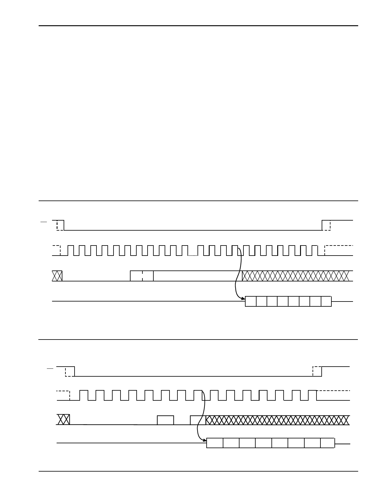
Figure 4. Read Instruction Timing
CS
0 1 2 3 4 5 6 7 8 9 10 20 21 22 23 24 25 26 27 28 29 30
SK
OPCODE
SI
0000001 1
BYTE ADDRESS*
SO
HIGH IMPEDANCE
*Please check the instruction set table for address
Note: Dashed Line= mode (1, 1) — — — —
Figure 5. RDSR Instruction Timing
DATA OUT
7 6 5 432 1 0
MSB
CS
SCK
0
1
2
3
4
5
6
7
8
9 10 11 12 13 14
OPCODE
SI
0
0
0
0
0
SO
HIGH IMPEDANCE
Note: Dashed Line= mode (1, 1) — — — —
1
0
1
DATA OUT
7
6
5
4
32
10
MSB
7
Doc. No. 1001, Rev. G
Share Link: 