HDLO-2416 гғҮгғјгӮҝгӮ·гғјгғҲгҒ®иЎЁзӨәпјҲPDFпјү - Broadcom Corporation
йғЁе“Ғз•ӘеҸ·
гӮігғігғқгғјгғҚгғігғҲиӘ¬жҳҺ
гғЎгғјгӮ«гғј
HDLO-2416 Datasheet PDF : 18 Pages
| |||
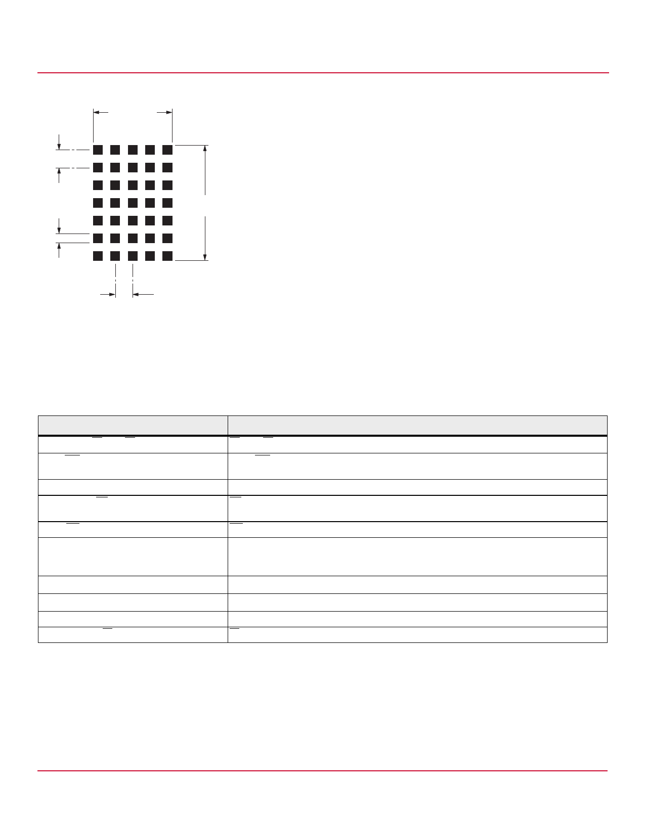
HDLx-2416 Series
Enlarged Character Font
0.80 (0.031)
TYP.
3.43 (0.135)
Data Sheet
5.08
(0.200)
0.25 (0.010)
TYP.
0.80 (0.031)
TYP.
NOTE
1. Unless otherwise specified, the tolerance on all dimensions is Вұ 0.254 mm (0.010 inch).
2. Dimensions are in mm (inches).
Electrical Description
Pin Function
Chip Enable (CE1 and CE2, pins 1 and 2)
Clear (CLR, pin 3)
Cursor Enable (CUE pin 4)
Cursor Select (CU, pin 5)
Write (WR, pin 6)
Address Inputs (A1 and A0, Pins 8 and 7)
Data Inputs (D0вҖ“D6, Pins 11-17)
VDD (pin 9)
GND (pin 10)
Blanking Input (BL, pin 18)
Description
CE1 and CE2 must be a logic 0 to write to the display.
When CLR is a logic 0 the ASCII RAM is reset to 20hex (space) and the Control Register/Attribute
RAM is reset to 00hex.
CUE determines whether the IC displays the ASCII or the Cursor memory. (1 = Cursor, 0 = ASCII).
CU determines whether data is stored in the ASCII RAM or the Attribute RAM/Control Register. (1
= ASCII, 0 = Attribute RAM/Control Register).
WR must be a logic 0 to store data in the display.
A0вҖ“A1 selects a specific location in the display memory.
Address 00 accesses the far right display location.
Address 11 accesses the far left location.
D0вҖ“D6 are used to specify the input data for the display.
VDD is the positive power supply input.
GND is the display ground.
BL is used to flash the display, blank the display or to dim the display.
Broadcom
- 10 -
Share Link: 