M34C02-RDW6T гғҮгғјгӮҝгӮ·гғјгғҲгҒ®иЎЁзӨәпјҲPDFпјү - STMicroelectronics
йғЁе“Ғз•ӘеҸ·
гӮігғігғқгғјгғҚгғігғҲиӘ¬жҳҺ
гғЎгғјгӮ«гғј
M34C02-RDW6T Datasheet PDF : 30 Pages
| |||
Signal description
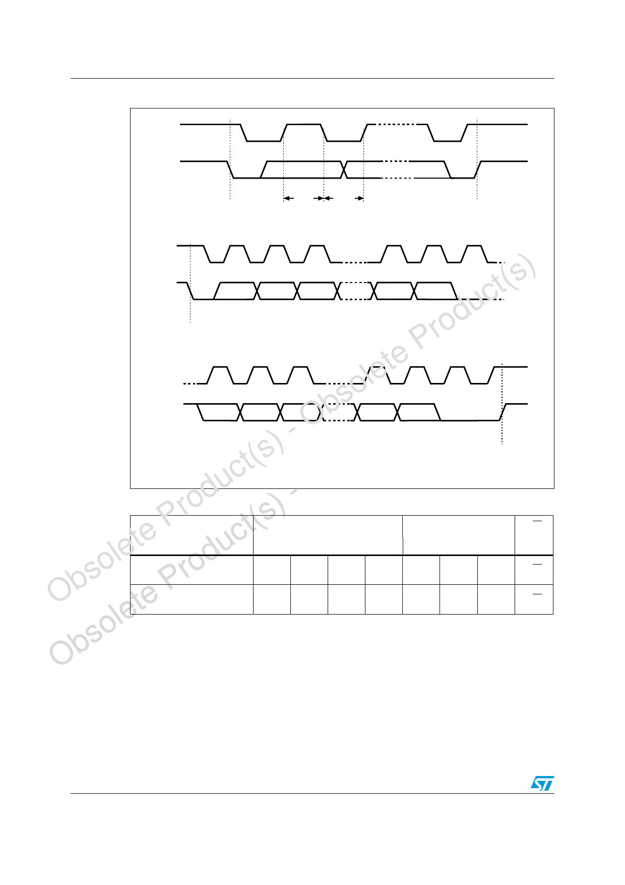
Figure 5. I2C bus protocol
SCL
SDA
START
Condition
SDA
Input
SDA
Change
M34C02-R
STOP
Condition
SCL
t(s) SDA
1
2
3
MSB
7
8
9
ACK
roduc START
) Condition
lete P uct(s SCL
bso Prod SDA
1
2
3
MSB
7
8
9
ACK
) - O lete STOP
t(s o Condition
c bs AI00792B
Produ t(s) - O Table 2.
Device select code
Device type Identifier(1)
Chip Enable address(2) RW
te c b7
b6
b5
b4
b3
b2
b1
b0
le du Memory area select code
so ro (two arrays)
1
0
1
0
E2
E1
E0
RW
b P Protection register select
O tecode
0
1
1
0
E2
E1
E0
RW
le1. The most significant bit, b7, is sent first.
Obso 2. E0, E1 and E2 are compared against the respective external pins on the memory device.
10/29
Share Link: 