MAX4473 データシートの表示(PDF) - Maxim Integrated
部品番号
コンポーネント説明
メーカー
MAX4473 Datasheet PDF : 9 Pages
| |||

Low-Cost, Low-Voltage, PA Power Control
Amplifier for GSM Applications
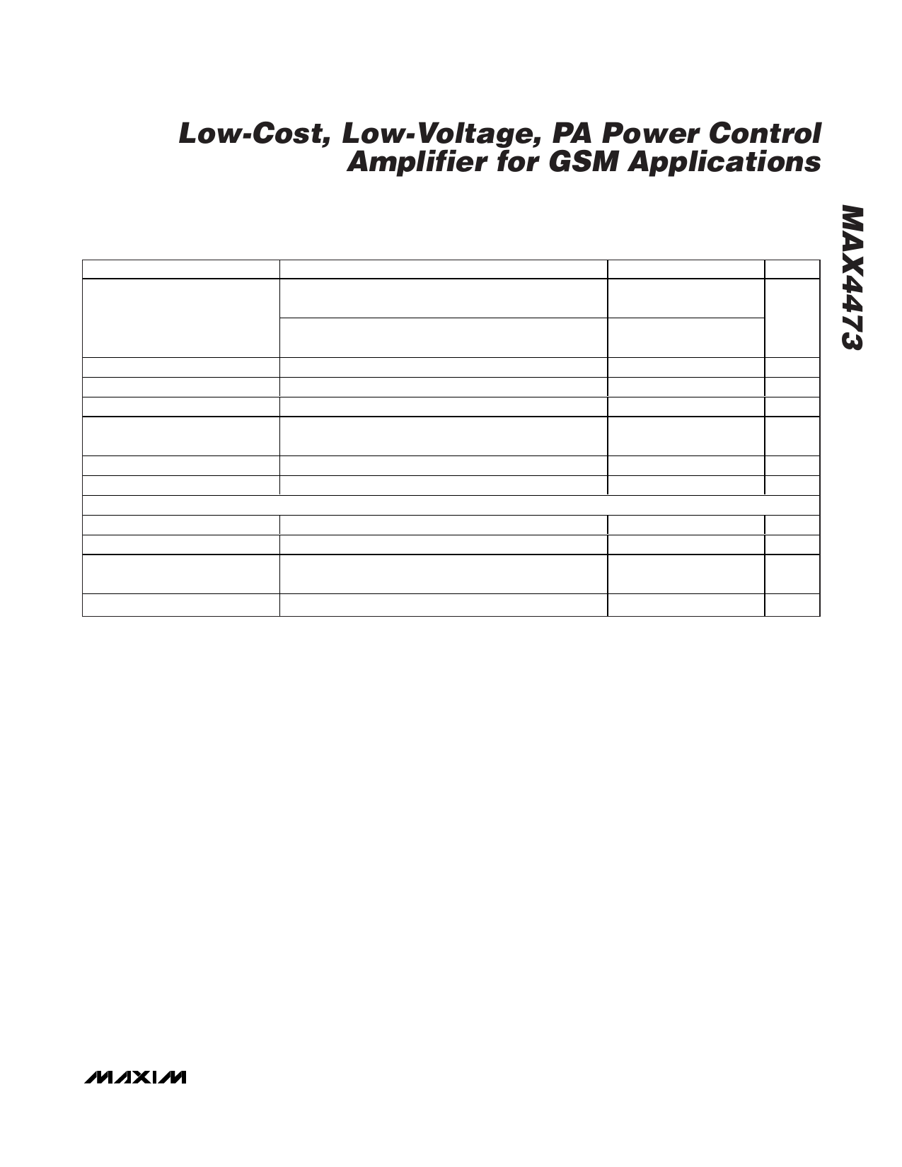
ELECTRICAL CHARACTERISTICS (continued)
(VCC = 2.7V to 6.5V, SHDN > 2.4V, MAX4473 test circuit, RG1 = RG2 = 1kΩ ±1%, RG3 = 2.5kΩ ±1%, RSENSE = 100Ω ±1%,
RL = 10kΩ, CL = 300pF, TA = TMIN to TMAX, unless otherwise noted. Typical values are at VCC = 6.0V, VPC = 1.0V, TA = +25°C.) (Note 1)
PARAMETER
CONDITIONS
MIN TYP MAX UNITS
Output Voltage Swing
RL = 10Ω to VCC / 2
RL = 500Ω to VCC / 2
0.15
0.5
VCC -
0.15
V
VCC -
0.5
Output Current Limit
Gain-Bandwidth Product
Phase Margin
VOUT = VCC / 2
RL = 10Ω, CL = 300pF, fo = 10kHz
RL = 10Ω, CL = 300pF
20
mA
2
MHz
60
degrees
Slew Rate
Measured from 30% to 70% of VOUT,
RL = 10Ω, CL = 300pF
1.8
V/µs
Capacitive-Load Stability
No sustained oscillations (Note 3)
Enable/Disable Time
From 50% of SHDN edge to VOUT = 1V, VPC = 2V
GAIN CONTROL BUFFER AND V-TO-I CONVERTER
0
300
pF
0.9
1.5
µs
PC Input Bias Current
SR3 Output Current Limit
GND < VPC < VCC - 0.15V
VPC < 2.55V, SR1 = SR2 = VCC
±0.04 ±1
µA
0.750
4
mA
VPC to VRG1 Ratio
Measure voltage across RG1,
0.3V < VPC < 2.55V (Note 4)
0.095 0.1 0.105 V/V
PC Input Bandwidth
Bandwidth from VPC to VRG1
2
MHz
Note 1: Limits over temperature are guaranteed by design.
Note 2: No output phase-reversal for input common-mode voltage range from GND to VCC. Common-mode range limited by voltage
drop across Q1 and RG3.
Note 3: Guaranteed by design.
Note 4: Error dependent on tolerance of RG1, RG2, and RG3. Specified with 0.1% tolerance resistors.
_______________________________________________________________________________________ 3