CXD3500R データシートの表示(PDF) - Sony Semiconductor
部品番号
コンポーネント説明
メーカー
CXD3500R Datasheet PDF : 73 Pages
| |||
CXD3500R
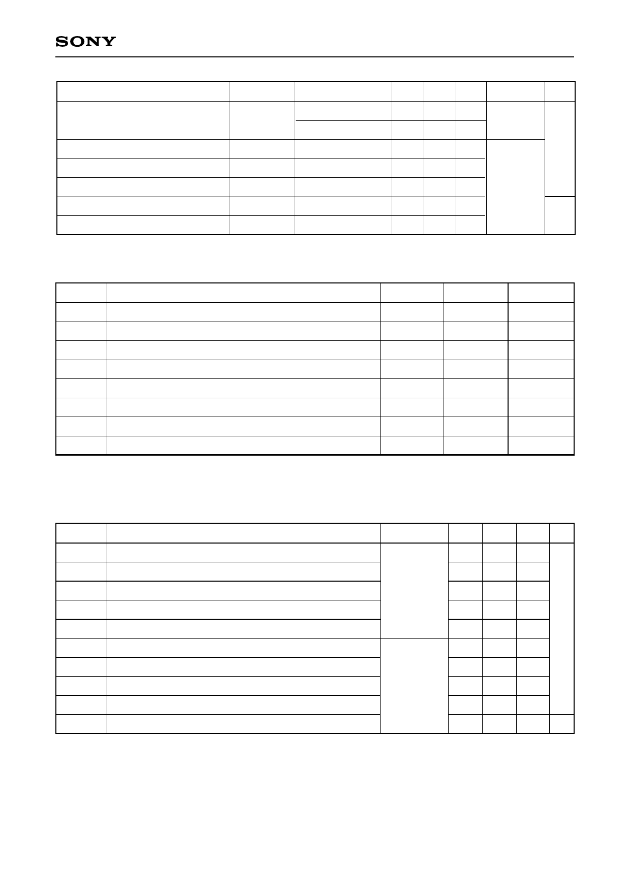
2. AC characteristics
(VDD = 5.0 ± 0.5V, VSS = 0V, Topr = –20 to +75°C)
Item
Symbol
Applicable pins Min. Typ. Max. Conditions Unit
Clock input cycle
CKI1
18.2
CKI2
18.2
Output rise time
tr
All outputs
20
ns
Output fall time
tf
All outputs
20
Cross-point time difference
∆t
HCK1, 2
–10
10 CL = 30pF
HCK1 Duty
HCK2 Duty
tH/(tH + tL) HCK1
48
52
%
tL/(tH + tL) HCK2
48
52
Note) The minimum value for the clock input cycle (CKI1) when using the built-in double-speed controller is 27ns.
3. Serial transfer AC characteristics
(VDD = 5.0 ± 0.5V, VSS = 0V, Topr = –20 to +75°C)
Symbol
Item
Min.
Typ.
Max.
ts0 SCTR setup time with respect to rise of SCLK
4Tns
ts1 SDAT setup time with respect to rise of SCLK
2Tns
th0 SCTR hold time with respect to rise of SCLK
4Tns
th1 SDAT hold time with respect to rise of SCLK
2Tns
tW1L SCLK L level pulse width
2Tns
tW1H SCLK H level pulse width
2Tns
tW2
5Tns
tW3
5Tns
T: Input clock cycle
Note) Consider the frequency at free running (no signal). When the above characteristic specification is not
satisfied at free running, IC operation including serial transfer is not guaranteed.
4. External clock input AC characteristics
(VDD = 5.0 ± 0.5V, VSS = 0V, Topr = –20 to +75°C)
Symbol
Item
Conditions Min. Typ. Max. Unit
ts0 HSYNC setup time with respect to rise of CKI1
4
th0 HSYNC hold time with respect to rise of CKI1
ts0 HSYNC setup time with respect to rise of CKI2
th0 HSYNC hold time with respect to rise of CKI2
SLCK∗1: H
7
CKPOL∗2: H 2
SLRS∗3: L
9
tWL/tWH CKI1,2 L/H level pulse width
6 T/2
ns
ts0 HSYNC setup time with respect to rise of CKI1
0
th0 HSYNC hold time with respect to rise of CKI1
ts0 HSYNC setup time with respect to rise of CKI2
th0 HSYNC hold time with respect to rise of CKI2
6
SLCK∗1: L
CKPOL∗2: H
0
8
tWL/tWH CKI1,2 L/H level pulse width
40 50 60 %
∗1, 2, 3: Serial data Add. 0A
T: Input clock cycle
Note) During external clock input, set serial data HR to L. The pulse synchronized to the horizontal sync signal is
generated by detecting the front edge of the horizontal sync signal and then resetting the internal PLL counter.
–6–
Share Link: 