LCX026ALG データシートの表示(PDF) - Sony Semiconductor
部品番号
コンポーネント説明
メーカー
LCX026ALG Datasheet PDF : 24 Pages
| |||
LCX026ALG
Input Signals
1. Input signal voltage conditions (VSS = 0V)
Item
Symbol
Min.
Typ.
Max.
Unit
H shift register input voltage (Low) VHIL
–0.5
0.0
HST, HCK1, HCK2, RGT (High) VHIH
4.5
5.0
0.4
V
5.5
V
V shift register input voltage (Low) VVIL
MODE1, MODE2, MODE3,
–0.5
0.0
BLK, VST, VCK, PCG,
ENB, DWN
(High) VVIH
4.5
5.0
0.4
V
5.5
V
Video signal center voltage
Video signal input range∗1
Common voltage of panel∗2
VVC
Vsig
Vcom
6.8
7.0
7.2
V
VVC – 4.5
7.0
VVC + 4.5 V
VVC – 0.5 VVC – 0.4 VVC – 0.3 V
Uniformity improvement signal
input voltage (PSIG)∗3
Vpsig
VVC ± 4.3 VVC ± 4.5 VVC ± 4.7 V
∗1 Input video signal shall be symmetrical to VVC.
∗2 The typical value of the common pad voltage may lower its suitable voltage according to the set
construction to use. In this case, use the voltage of which has maximum contrast as typical value.
When the typical value is lowered, the maximum and minimum values may lower.
∗3 Input a uniformity improvement signal PSIG in the same polarity with video signals SIG1 to 6 and which is
symmetrical to VVC. Also, the rising and falling of PSIG are synchronized with the rising of PCG pulse, and
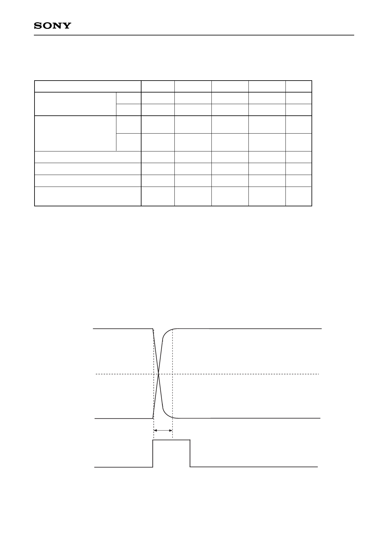
the rise time trPSIG and fall time tfPSIG are suppressed within 800ns (as shown in a diagram below).
The optimum input voltage of PSIG may be changed according as drive conditions of the drive side.
Input waveform of uniformity improvement signal PSIG
90%
PSIG
VVC
PCG
10%
trPSIG
tfPSIG
Level Conversion Circuit
The LCX026ALG has a built-in level conversion circuit in the clock input unit on the panel. The input signal
level increases to HVDD or VVDD. The VCC of external ICs are applicable to 5 ± 0.5V.
–5–
Share Link: 