LCX026ALE データシートの表示(PDF) - Sony Semiconductor
部品番号
コンポーネント説明
メーカー
LCX026ALE Datasheet PDF : 24 Pages
| |||
LCX026ALE
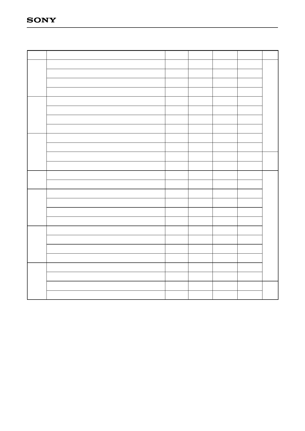
2. Clock timing conditions (Ta = 25°C)
(SVGA mode: fHCKn = 4.0MHz, fVCK = 24.0kHz)
Item
Symbol Min.
HST
HCK
VST
Hst rise time
Hst fall time
Hst data set-up time
Hst data hold time
Hckn rise time∗4
Hckn fall time∗4
Hck1 fall to Hck2 rise time
Hck1 rise to Hck2 fall time
Vst rise time
Vst fall time
Vst data set-up time
trHst
—
tfHst
—
tdHst
50
thHst
50
trHckn
—
tfHckn
—
to1Hck –15
to2Hck –15
trVst
—
tfVst
—
tdVst
5
Vst data hold time
thVst
5
Vck rise time
VCK
Vck fall time
trVck
—
tfVck
—
Enb rise time
trEnb
—
Enb fall time
ENB
Vck rise/fall to Enb rise time
tfEnb
—
tdEnb
400
Enb pulse width
twEnb 2400
Pcg rise time
trPcg
—
Pcg fall time
PCG
Pcg rise to Vck rise/fall time
tfPcg
—
toVck
900
Pcg pulse width
twPcg 1100
Blk rise time
trBlk
—
BLK∗5 Blk fall time
Blk fall to Vst rise time
tfBlk
—
toVst
32
Blk pulse width
twBlk
20
∗4 Hckn means Hck1 and Hck2.
∗5 Blk is the timing during SVGA mode (fHckn = 4.0MHz, fVck = 24.0kHz).
Typ.
—
—
60
60
—
—
0
0
—
—
10
10
—
—
—
—
500
2500
—
—
1000
1200
—
—
33
21
Max. Unit
30
30
70
70
30
ns
30
15
15
100
100
15
µs
15
100
100
100
100
600
2600
ns
30
30
1100
1300
100
100
34
µs
22
–6–
Share Link: 