CH1804 データシートの表示(PDF) - Cermetek Microelectronics
部品番号
コンポーネント説明
メーカー
CH1804 Datasheet PDF : 5 Pages
| |||
Cermetek Microelectronics, Inc.
occur in an installation, the CH1804/9 will only detect
when TIP and RING are both cut. However,
regardless of the installation wiring, the
CH1804A/CH1809A products will always detect an off-
hook condition. If it is required to detect and identify
which line (i.e., either TIP or RING) has been cut, then
a voltage sense device is required, such as the
Cermetek CH1808 line status detector product.
APPLICATION RECOMENDATIONS
Failure to Detect Cut Line. When using either the
CH1804 or the CH1809 products, external leakage
and capacitance on TIP and RING must be minimized.
Differential leakage to TIP and RING in excess of 0.1
microamperes may appear as a central office battery
voltage thereby causing the CH1804/9 to fail to detect
a cut line. Additionally, Common mode leakage to TIP
and RING in excess of 1 microampere is also
undesirable. Thus, the circuit board layout and
external wiring for TIP and RING must be well
insulated.
Off-Hook Indication Delay. Capacitance on TIP and
RING should be minimized as it could retain charge
after a transition and appear as a central office battery
voltage. This will delay detection of an Off-Hook
condition for many tens of seconds. The input
impedance of the detector circuit is approximately 10M
ohms to ground, and the capacitance may have to be
discharged for 3 or 4 time constants to indicate a
detection depending on initial conditions. Thus, it
would be desirable to keep capacitance well below
1µF to keep the delay from exceeding ten seconds.
Normal Operation. If the CH1804/A or the CH1809/A
is the only device on the telephone line, leakage and
differential capacitance will tend not to affect normal
operation, since the line capacitance in the central
office or the local loop are minimal. The more devices
that share a given local loop, such as modems and
extension telephones, the greater the capacitance and
leakage possibilities. Sources of capacitance, when
On-Hook, include ring detection circuits in modems.
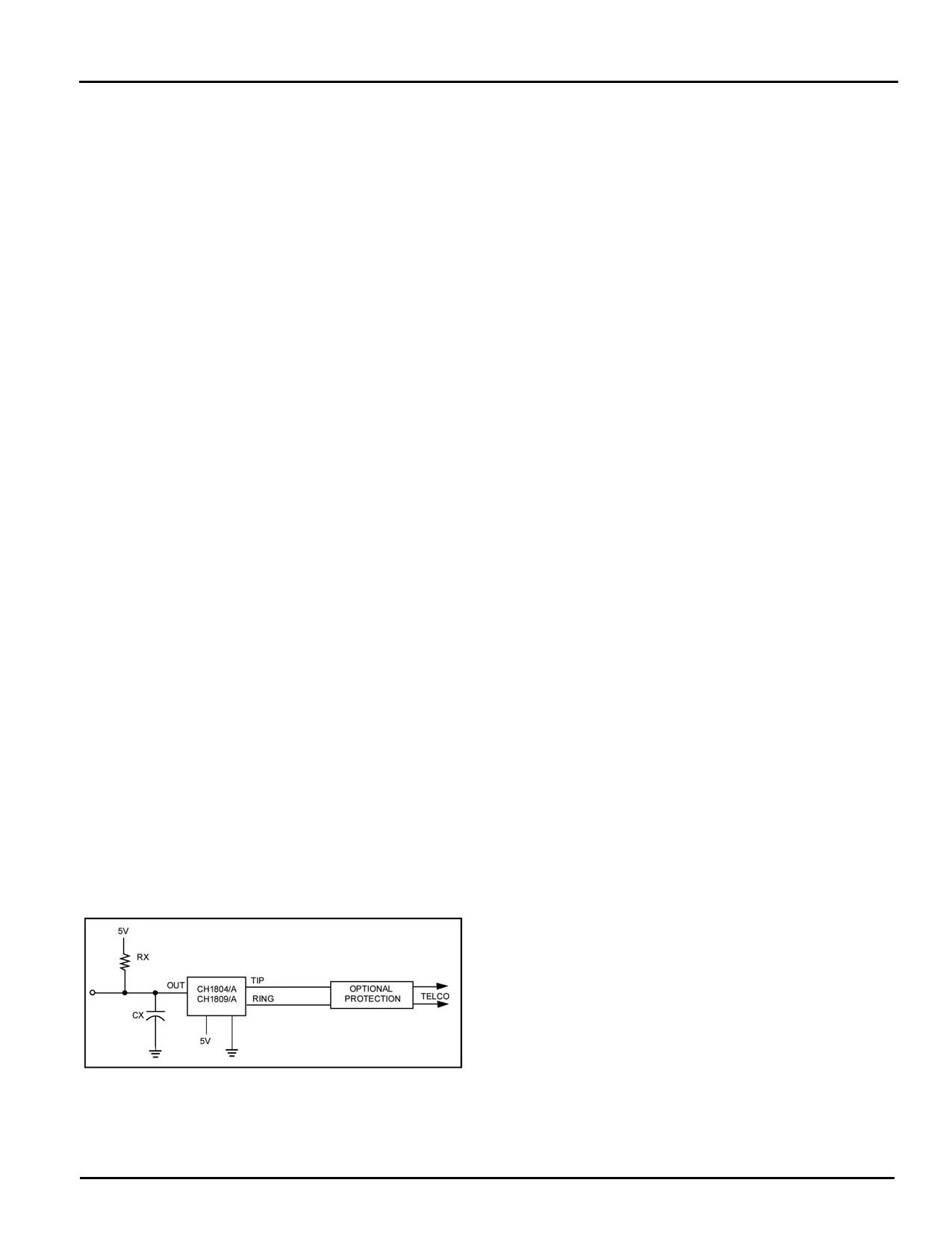
Figure 2. Application Diagram indicating external
components to increase output drive, decrease
false line cut indications and provide additional
overvoltage protection.
CH1804/A and CH1809/A
Potential False Indication. The CH1804/A and
CH1809/A products reside on the telephone line and,
as such, are subject to transients produced by
electrical discharge and ring voltage transitions.
These may cause momentary false Cut Line or Off-
Hook indications. The use of additional external
capacitance on the output may be required to reduce
these false indications. The capacitance value to add
to each output should be determined by appropriate
analysis and testing for the particular application.
Cermetek recommends that the outputs be level
detected as opposed to edge detected to minimize
false indications on excessively noisy lines. Referring
to Figure 2, typical values are 0.1µf and 30K ohms for
CX and RX, respectively.
SUPPLEMENTAL PROTECTION
If the CH1804A/9A products are being used on
telephone lines that are prone to high voltage
transients, an FCC Part 15 A/B suppressor may be
required. This consists of 1.25 A fuses in both TIP and
RING lines and a 350V voltage suppressor between
TIP and RING for transient protection. A ferrite bead
inductor and 0.1µF capacitor (1500V) to ground may
also be required for EMI/RFI suppression. See
Cermetek Application Note # 126. If the CH1804A/9A
is being used with another Cermetek device where the
supplemental protection is already planned for or
available, the CH1804A/9A can share the protection if
a parallel connection to the TIP and RING pins is
made in front of the protective network.
DESIGN
CONSIDERATION
FOR
FCC
CONFORMANCE
The CH1804A/9A products include circuits that couple
to the phone line and provide FCC required isolation
and protection. The following guidelines should be
followed to maintain the conveyed FCC Part 68
registration:
1) CH1804A/9A must be mounted away from
hazardous voltages.
2) Connection of the CH1804A/9A devices to PSTN
lines should be made through a standard RJ-11C
jack or another approved connector device.
3) Circuit board traces to the CH1804A/9A TIP and
RING pins must have a spacing of greater than
0.10 inch from all adjacent traces. TIP and RING
traces should have a width of 0.020 inches.
4) TIP and RING traces should be as short as
possible to prevent coupling to other signals lines.
Mount the CH1804A/9A as close to the telephone
line connection as possible.
2003 Cermetek Microelectronics, Inc.
Page 2
Document No. 607-0015 Revision C (05/03)
Share Link: 