MJD44H11 データシートの表示(PDF) - Powerex
部品番号
コンポーネント説明
メーカー
MJD44H11 Datasheet PDF : 7 Pages
| |||
Powerex, Inc., 200 E. Hillis Street, Youngwood, Pennsylvania 15697-1800 (724) 925-7272
M57161L-01
Hybrid IC for IGBT Gate Driver
M57161L-01
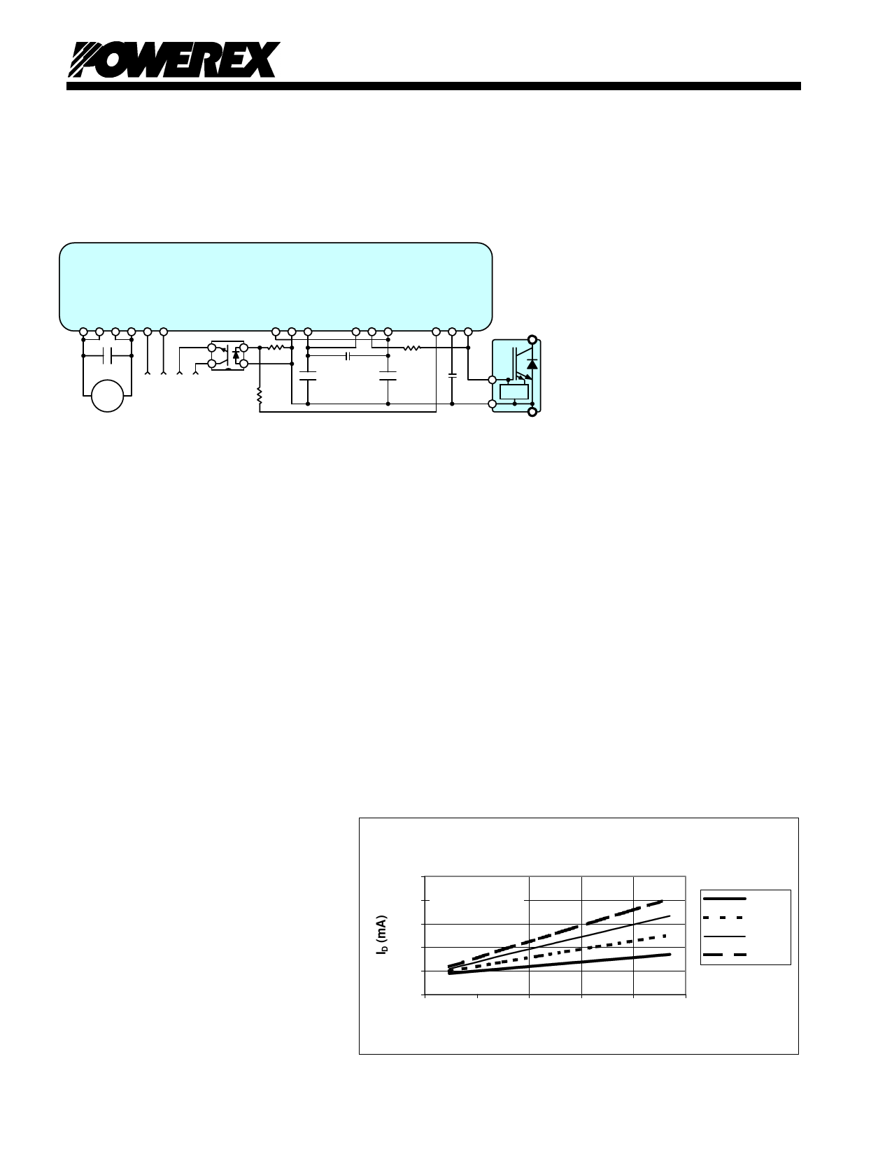
Figure 5 M57161L-01 Typical Application Circuit
sufficiently high ripple current rating.
The example circuit in Figure 5 uses
a 150µF low impedance type
electrolytic for the input decoupling
M57161L-01
capacitor.
The driver’s built-in DC-DC
1
6
17 19
22 24
27 29
converter produces isolated +17.4V
and -6.5V outputs at pins 19 and 17
+
150µF
+ VD
+ - FO
Vin
3.3k
+
2.2µF
RG
470Ω
150µF 150µF +
G
CTRIP
RTC
E
IGBT Module
with respect to the common pin 18.
These voltages are supplied to
driver’s output stage on pins 22 and
24 to provide high current gate drive
with on and off driving voltages of
+15.5V and –5V. In order to deliver
the pulse current necessary for efficient switching, the output of the isolated DC-DC converter (pins 17, 18 and 19)
must be decoupled using a combination of low impedance electrolytic and film capacitors. In Figure 5 the 150µF
low impedance electrolytics and a 2.2µF stacked film or multi-layer ceramic are included for this purpose. These
capacitors should be located as close as possible to the pins of the hybrid gate driver. When driving small
modules it is usually acceptable to use smaller capacitors provided that that they have sufficient ripple current
capability and low enough impedance. However, very large modules and parallel module applications may require
500µF or more to achieve low enough impedance and high enough ripple current capability.
The series gate resistor (RG) should be selected based on the application requirements and module type being
used. Details for selecting RG can be found in Powerex IGBT module application notes. The minimum allowable
RG for the M57161L-01 is 2.2Ω. If a smaller value is desired, a booster stage must be added. (See Section 7.)
The back-to-back zener diodes from G to E that are normally recommended are not required with F-Series IGBT
modules because they are included as part of the modules internal RTC circuit.
Pin 28 is used to adjust the RTC detection time and total shut-down time. This adjustment was described in
detail in Section 3. To extend the trip time, CTRIP can be connected as shown in Figure 5. This capacitor should
be located as close as possible to the pins of the gate driver.
Pin 27 is an active low fault status signal. When a fault (short circuit or undervoltage) is detected this pin is
pulled down to the VEE supply. In Figure 5 a low speed optocoupler is utilized to provide isolation of the fault
feedback signal. The optocoupler is connected from the common of the isolated power supply (pin 18) to the fault
signal pin using a 470Ω current limiting resistor. When a fault occurs a current of approximately 10mA will flow in
the optocoupler’s LED. A 3.3kΩ resistor connected across the opto’s photodiode helps to improve noise immunity.
6. Control Power Supply Requirements
Figure 6 Supply Current versus Gate Charge
The control power supply current
required for the M57161L-01 is primarily a
function of the gate charge (QG) of the
IGBT module being driven and the
500
400 VGE = +15V/-5V
switching frequency. Figure 6 shows the
300
15V control power supply current (ID) as a
function of IGBT module gate charge for
200
various switching frequencies. This curve
100
provides an estimate of the required
current. The actual current will vary
depending on the operating conditions of
the IGBT module. To accommodate these
0
0
2
4
6
8
10
QG (µC)
variations, it is recommended that the 15V
supply be designed to provide 150% - 200% of the value indicated in Figure 6.
5 kHz
10 kHz
15 kHz
20 kHz
6
Share Link: 