TNY289KG データシートの表示(PDF) - Power Integrations, Inc
部品番号
コンポーネント説明
メーカー
TNY289KG
Power Integrations, Inc

TNY289KG Datasheet PDF : 26 Pages
| |||
TNY284-290
BR1
2KBP10M
1000 V
L1
10 mH
RT1
6Ω
C1
100 nF
F1 275 VAC
5A
90 - 295
VAC
C2
68 µF
450 V
C3
2.2 nF
1 kV
VR1
P6KE150A
R12
2 MΩ
R13
2 MΩ
R1
22 Ω
1/2 W
D1
UF4006-E3
D
TinySwitch-4
U1
TNY290PG
S
EN/UV
BP/M
C16
100 nF
100 V
C13
2.2 nF
250 VAC
1 9,10
R3 C5
4.7 Ω 1.5 nF
1/2 W 100 V
C6, C7
1500 µF
10 V
D4
STPS30L60CT
7,8
4
3
5
T1
EE22
R15
1.5 MΩ
1/8 W
D3
1N4937
R2
8.2 Ω
C4
100 µF
50 V
VR2
1N5254
27 V
R4
30 kΩ
1/8 W
C9
10 µF
16 V
U3
PC817
C11
2.2 µF
50 V
C8
1000 µF
10 V
L2
2.2 µH
R9
47 Ω
R6
10 kΩ
1%
5 V, 4 A
RTN
R8
1 kΩ
1/8 W
R14 C10
3.3 kΩ 47 nF
1/8 W 100 V
U2
TL431
R7
10 kΩ
1%
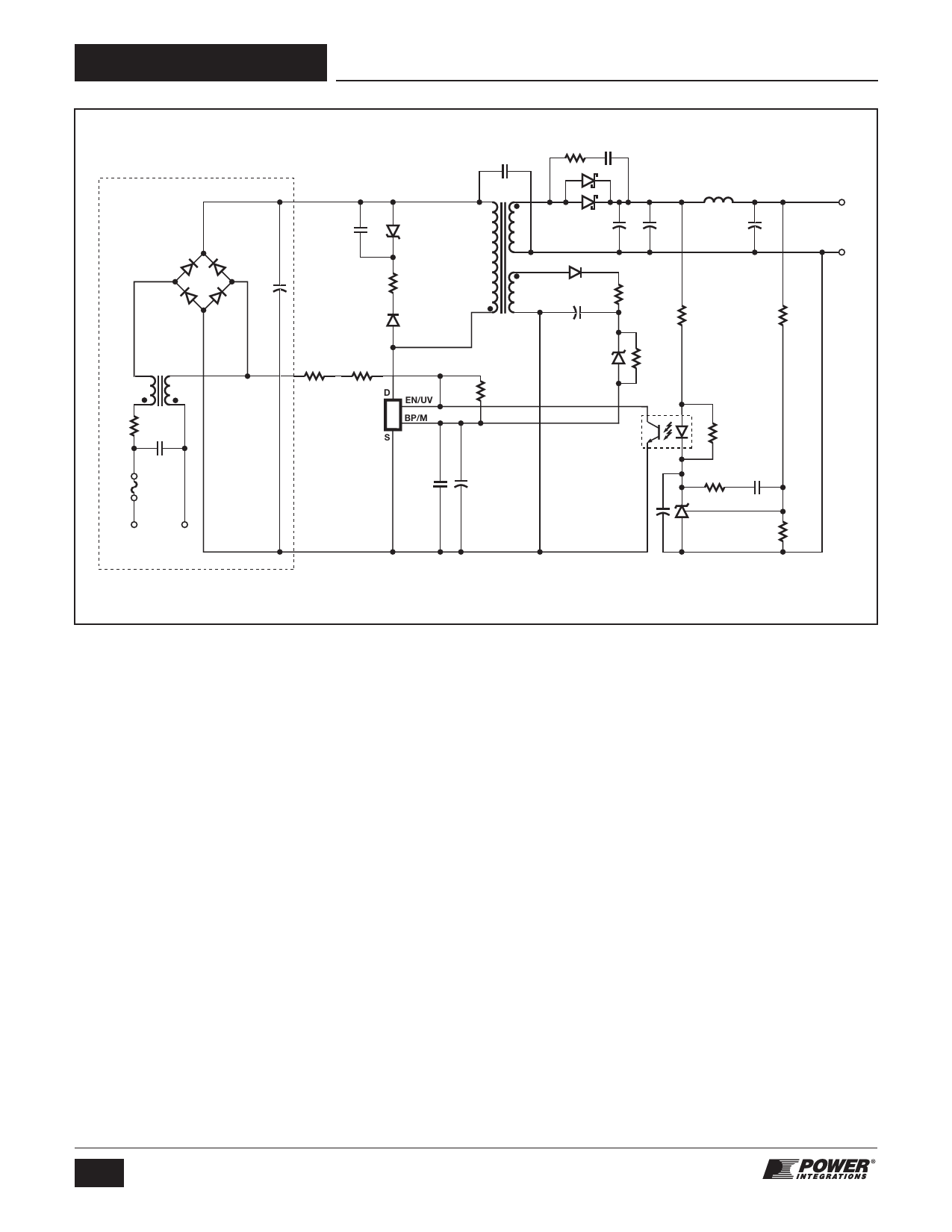
PI-6559-062012
In a PC standby application input stage
will be part of main power supply input
Figure 16. TNY290PG, 5 V, 4 A Universal Input Power Supply.
Applications Example
The circuit shown in Figure 16 is a low cost, high efficiency,
flyback power supply designed for 5 V, 4 A output from
universal input using the TNY290PG.
The supply features undervoltage lockout, primary sensed
output overvoltage latching shutdown protection, high
efficiency (>80%), and very low no-load consumption (<50 mW
at 265 VAC). Output regulation is accomplished using a simple
Zener reference and optocoupler feedback.
The rectified and filtered input voltage is applied to the primary
winding of T1. The other side of the transformer primary is
driven by the integrated MOSFET in U1. Diode D1, C3, R1, and
VR1 comprise the clamp circuit, limiting the leakage inductance
turn-off voltage spike on the DRAIN pin to a safe value.
The output voltage is regulated by TL431 U2. When the output
voltage ripple exceeds the sum of the U2 (CATHODE D6) and
optocoupler LED forward drop, current will flow in the
optocoupler LED. This will cause the transistor of the
optocoupler to sink current. When this current exceeds the
ENABLE pin threshold current the next switching cycle is
inhibited. When the output voltage falls below the feedback
threshold, a conduction cycle is allowed to occur and, by
adjusting the number of enabled cycles, output regulation is
maintained. As the load reduces, the number of enabled
cycles decreases, lowering the effective switching frequency
and scaling switching losses with load. This provides almost
constant efficiency down to very light loads, ideal for meeting
energy efficiency requirements.
As the TinySwitch-4 devices are completely self-powered, there
is no requirement for an auxiliary or bias winding on the
transformer. However by adding a bias winding, the output
overvoltage protection feature can be configured, protecting the
load against open feedback loop faults.
When an overvoltage condition occurs, such that bias voltage
exceeds the sum of VR2 and the BYPASS/MULTIFUNCTION
(BYPASS/MULTI-FUNCTIONAL) pin voltage, current begins to
flow into the BYPASS/MULTI-FUNCTIONAL pin. When this
current exceeds ISD the internal latching shutdown circuit in
TinySwitch-4 is activated. This condition is reset when the
ENABLE/UNDERVOLTAGE pin current flowing through R12 and
R13 drop below 18.75 mA each AC line half-cycle. The
configuration of Figure 16 is therefore non-latching for an
overvoltage fault. Latching overvoltage protection can be
achieved by connecting R12 and R13 to the positive terminal of
C2, at the expense of higher standby consumption. In the
example shown, on opening the loop, the OVP trips at an
output of 17 V.
For lower no-load input power consumption, the bias winding
may also be used to supply the TinySwitch-4 device. Resistor
8
Rev. A 09/12
www.powerint.com
Share Link: