AT91SAM データシートの表示(PDF) - Atmel Corporation
部品番号
コンポーネント説明
メーカー
AT91SAM Datasheet PDF : 1185 Pages
| |||
6.1 Memory Mapping
A first level of address decoding is performed by the AHB Bus Matrix, i.e., the implementation of the Advanced
High performance Bus (AHB) for its Master and Slave interfaces with additional features.
Decoding breaks up the 4 Gbytes of address space into 16 banks of 256 Mbytes. The banks 1 to 6 are directed to
the EBI that associates these banks to the external chip selects NCS0 to NCS5.
The bank 7 is directed to the DDRSDRC0 that associates this bank to DDR_NCS chip select and so dedicated to
the 4-port DDR2/ LPDDR controller.
The bank 0 is reserved for the addressing of the internal memories, and a second level of decoding provides 1
Mbyte of internal memory area. The bank 15 is reserved for the peripherals and provides access to the Advanced
Peripheral Bus (APB).
Other areas are unused and performing an access within them provides an abort to the master requesting such an
access.
6.2 Embedded Memories
6.2.1
Internal SRAM
The SAM9G45 product embeds a total of 64Kbytes high-speed SRAM split in 4 blocks of 16 Kbytes connected to
one slave of the matrix. After reset and until the Remap Command is performed, the four SRAM blocks are contig-
uous and only accessible at address 0x00300000. After Remap, the SRAM also becomes available at address
0x0.
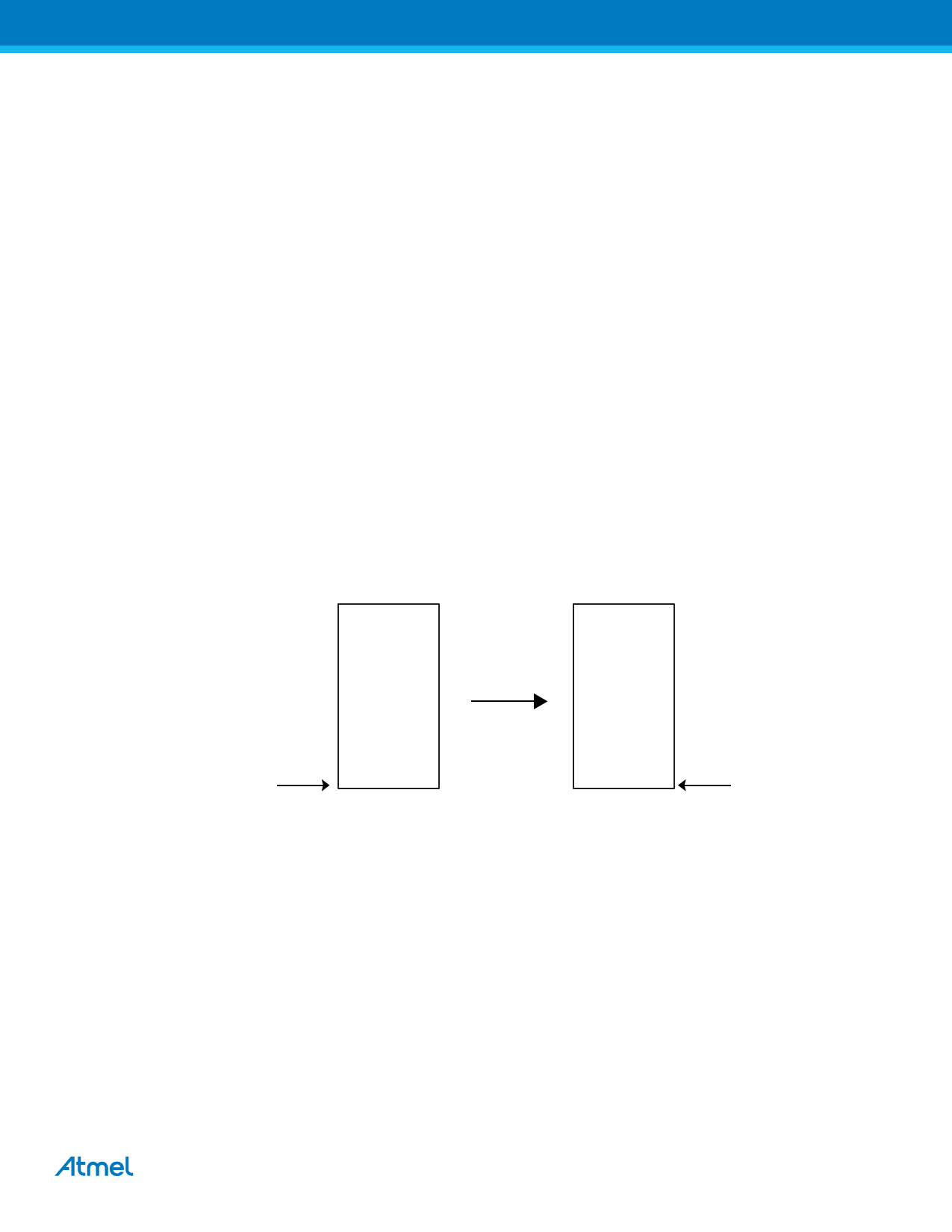
Figure 6-2. Internal SRAM Reset
RAM
RAM
Remap
64K
64K
0x00300000
0x00000000
The SAM9G45 device embeds two memory features. The processor Tightly Coupled Memory Interface (TCM) that
allows the processor to access the memory up to processor speed (PCK) and the interface on the AHB side allow-
ing masters to access the memory at AHB speed (MCK).
A wait state is necessary to access the TCM at 400 MHz. Setting the bit NWS_TCM in the bus Matrix TCM Config-
uration Register of the matrix inserts a wait state on the ITCM and DTCM accesses.
6.2.2
TCM Interface
On the processor side, this Internal SRAM can be allocated to two areas.
• Internal SRAM A is the ARM926EJ-S Instruction TCM. The user can map this SRAM block anywhere in the
ARM926 instruction memory space using CP15 instructions and the TCR configuration register located in the
Chip Configuration User Interface. This SRAM block is also accessible by the ARM926 Masters and by the AHB
Masters through the AHB bus
SAM9G45 [DATASHEET] 16
6438K–ATARM–12-Feb-13
Share Link: 