IN74LS07N データシートの表示(PDF) - IK Semicon Co., Ltd
部品番号
コンポーネント説明
メーカー
IN74LS07N Datasheet PDF : 4 Pages
| |||
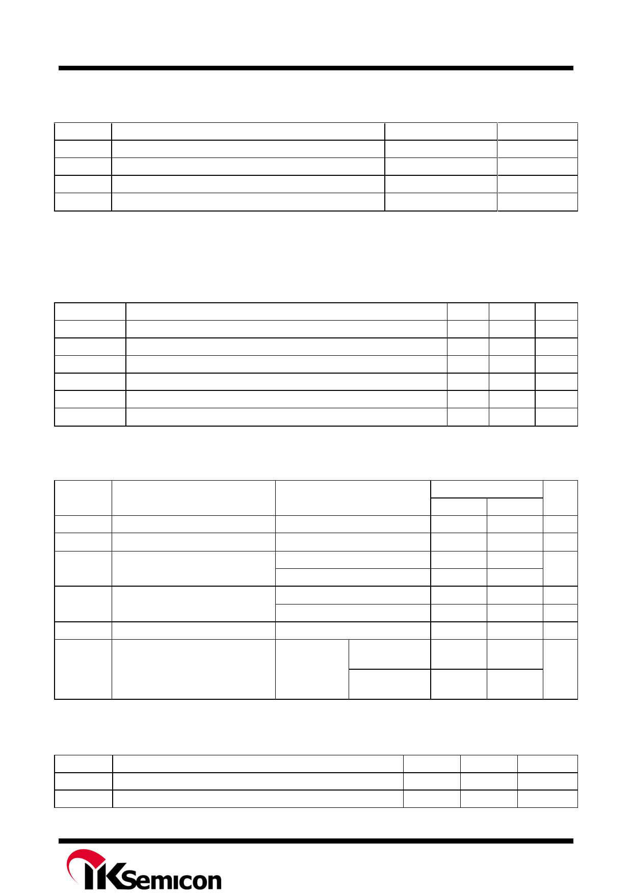
IN74LS07
MAXIMUM RATINGS*
Symbol
Parameter
Value
Unit
VCC
VIN
VOUT
Tstg
Supply Voltage
Input Voltage
Output Voltage
Storage Temperature Range
7.0
V
5.5
V
30
V
-65 to +150
°C
*Maximum Ratings are those values beyond which damage to the device may occur.
Functional operation should be restricted to the Recommended Operating Conditions.
RECOMMENDED OPERATING CONDITIONS
Symbol
VCC
VIH
VIL
VOH
IOL
TA
Parameter
Supply Voltage
High Level Input Voltage
Low Level Input Voltage
High Level Output Voltage
Low Level Output Current
Ambient Temperature Range
Min Max Unit
4.75 5.25
V
2.0
V
0.8
V
30
V
40
mA
0
+70
°C
DC ELECTRICAL CHARACTERISTICS over full operating conditions
Symbol
VIK
IOH
VOL
Parameter
Input Clamp Voltage
High Level Output Current
Low Level Output Voltage
IIH
High Level Input Current
IIL
Low Level Input Current
ICC
Supply Current
Test Conditions
VCC = 4.75, IIN = -18 mA
VCC = 4.75, VOH= 5.25
VCC = 4.75, IOL = 16 mA
VCC = 4.75, IOL = 40 mA
VCC = 5.25, VIN = 2.7 V
VCC = 5.25, VIN = 5.5 V
VCC = 5.25, VIN = 0.4 V
VCC = 5.25
Total with
outputs high
Total with
outputs low
Guaranteed Limit
Min
Max Unit
-1.5
V
250
μA
0.4
V
0.7
20
μA
1
mA
-0.2
mA
14
mA
45
AC ELECTRICAL CHARACTERISTICS
(TA = 25°C, VCC = 5.0 V, CL = 15 pF, RL = 100 Ω,tr = 15 ns, tf = 6.0 ns)
Symbol
tPLH
tPHL
Parameter
Propagation Delay, Input A to Output Y
Propagation Delay, Input A to Output Y
Min
Max
Unit
10
ns
30
ns
Rev. 01
Share Link: 