LD3985G44R データシートの表示(PDF) - STMicroelectronics
部品番号
コンポーネント説明
メーカー
LD3985G44R
STMicroelectronics

LD3985G44R Datasheet PDF : 14 Pages
| |||
LD3985 SERIES
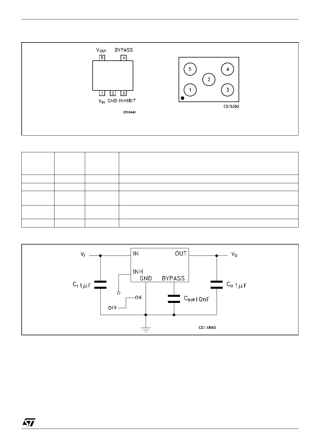
Figure 2: Connection Diagram (top view for SOT and TSOT, top through view for Flip-Chip)
TSOT23-5L/SOT23-5L
Flip-Chip
Table 4: Pin Description
Pin N°
SOT23-5L/
TSOT23-5L
1
2
3
Pin N°
Flip-Chip
4
2
1
4
5
5
3
Symbol
Name and Function
VI
GND
VINH
BYPASS
VO
Input Voltage of the LDO
Common Ground
Inhibit Input Voltage: ON MODE when VINH ≥ 1.2V, OFF MODE when VINH ≤
0.4V (Do not leave floating, not internally pulled down/up)
Bypass Pin: Connect an external capacitor (usually 10nF) to minimize noise
voltage
Output Voltage of the LDO
Figure 3: Typical Application Circuit
3/14
Share Link: