TDA3616 データシートの表示(PDF) - Philips Electronics
部品番号
コンポーネント説明
メーカー
TDA3616 Datasheet PDF : 20 Pages
| |||
Philips Semiconductors
Multiple voltage regulator with battery
detection
Objective specification
TDA3616
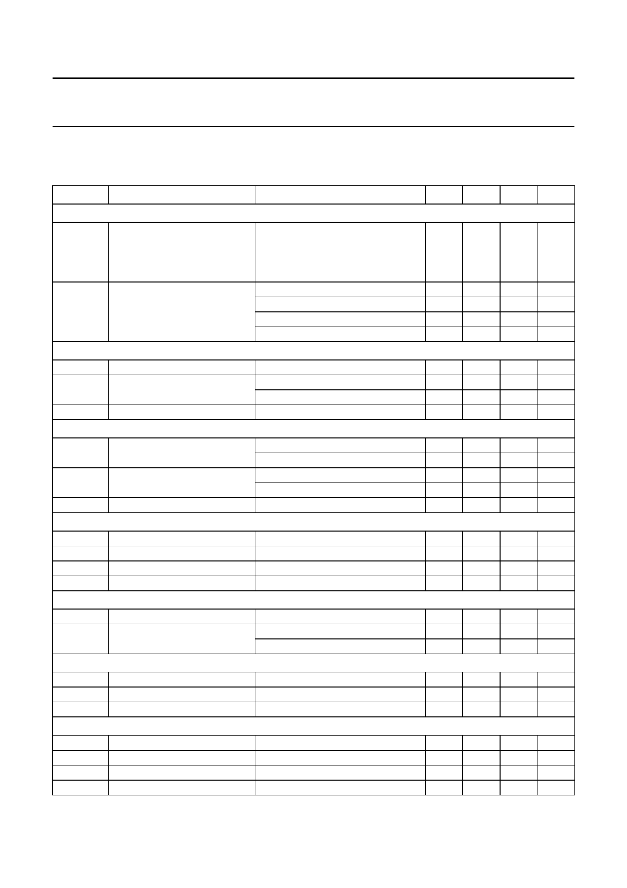
CHARACTERISTICS
VP = 14.4 V; IREG = 0.5 mA; −40 °C < Tamb < +105 °C; measurements taken in test circuit of Fig.7; unless otherwise
specified.
SYMBOL
PARAMETER
CONDITIONS
MIN. TYP. MAX. UNIT
Supply
VP
Iq
supply voltage
operating
jump start
load dump protection
quiescent supply current
Schmitt trigger for regulator and reset 1
Vth(r)
Vth(f)
rising threshold voltage
falling threshold voltage
Vhys
hysteresis voltage
Schmitt trigger for battery detection
Vth(r)
rising threshold voltage
regulator on; note 1
t ≤ 10 minutes
t ≤ 50 ms; tr ≥ 2.5 ms
VP = 12.4 V; Tamb = 25 °C; note 2
VP = 12.4 V; note 2
VP = 14.4 V; note 2
VP = 50 V; load dump
RL(REG) = 1 kΩ
IREG = 5 mA
IREG = 30 mA
Tamb = 25 °C
Vth(f)
falling threshold voltage
Tamb = 25 °C
Vhys
hysteresis voltage
Schmitt trigger for reset 2
Vth(r)
Vth(f)
Vhys
∆Vtrack
rising threshold voltage
falling threshold voltage
hysteresis voltage
voltage tracking with VREG
Reset 1 and reset 2 buffers
Isink(L)
Rpu(int)
LOW-level sink current
internal pull-up resistance
note 3
note 3
Isink = 0 mA; note 4
VRES ≤ 0.5 V; note 3
Tamb = 25 °C
Reset delay
Rpu(int)
Vth(r)
td
internal pull-up resistance
rising threshold voltage
delay time
Battery buffer
VOL
LOW-level output voltage
VOH
HIGH-level output voltage
IOL
LOW-level output current
IOH
HIGH-level output current
Tamb = 25 °C; note 5
Cd = 100 nF; note 6; see Fig.9
II = 0 mA
Io = 5 µA; note 7
VOL ≤ 0.5 V
VOH ≥ 4 V; see Fig.6
5.6 14.4 25
V
−
−
30
V
−
−
50
V
−
95
120 µA
−
95
125 µA
−
100 −
µA
−
5
20
mA
6.2 7.5 8.1 V
2.1 2.4 2.7 V
−
2.25 −
V
−
5.1 −
V
2.0 2.1 2.2 V
2.0 2.1 2.25 V
1.9 2.0 2.1 V
1.9 2.0 2.15 V
−
0.1 −
V
4.55 4.8 5.05 V
4.5 4.75 5.0 V
−
0.05 −
V
−65 0
+65 mV
2
15
−
mA
2.2 3.1 4.0 kΩ
1.9 3.1 4.6 kΩ
−
47
−
kΩ
1.4 2.0 2.8 V
−
2.6 −
ms
0
0.05 0.5 V
−
5.0 5.2 V
0.2 0.5 −
mA
1
12
−
mA
2000 Jan 14
7
Share Link: 