MC100LVE111 データシートの表示(PDF) - Motorola => Freescale
部品番号
コンポーネント説明
メーカー
MC100LVE111 Datasheet PDF : 5 Pages
| |||
MC100LVE111
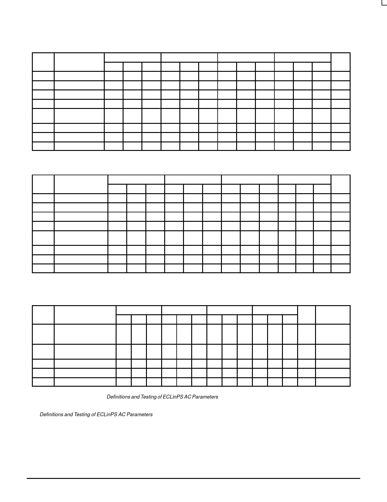
ECL DC CHARACTERISTICS
–40°C
0°C
25°C
85°C
Symbol
Characteristic
Min Typ Max Min Typ Max Min Typ Max Min Typ Max Unit
VOH
VOL
VIH
VIL
VBB
Output HIGH Voltage –1.025 –0.955 –0.880 –1.025 –0.955 –0.880 –1.025 –0.955 –0.880 –1.025 –0.955 –0.880 V
Output LOW Voltage –1.810 –1.705 –1.620 –1.810 –1.705 –1.620 –1.810 –1.705 –1.620 –1.810 –1.705 –1.620 V
Input HIGH Voltage
–1.165
–0.880 –1.165
–0.880 –1.165
–0.880 –1.165
–0.880 V
Input LOW Voltage
–1.810
–1.475 –1.810
–1.475 –1.810
–1.475 –1.810
–1.475 V
Output Reference
Voltage
–1.38
–1.26 –1.38
–1.26 –1.38
–1.26 –1.38
–1.26
V
VEE
IIH
IEE
Power Supply Voltage –3.0
–3.8 –3.0
–3.8 –3.0
–3.8 –3.0
Input HIGH Current
150
150
150
Power Supply Current
55
66
55
66
55
66
65
–3.8
V
150
µA
78
mA
PECL DC CHARACTERISTICS
–40°C
0°C
25°C
85°C
Symbol
VOH
VOL
VIH
VIL
VBB
Characteristic
Output HIGH Voltage1
Output LOW Voltage1
Input HIGH Voltage1
Input LOW Voltage1
Output Reference Volt-
age1
Min Typ Max Min Typ Max Min Typ Max Min Typ Max Unit
2.275 2.345 2.420 2.275 2.345 2.420 2.275 2.345 2.420 2.275 2.345 2.420 V
1.490 1.595 1.680 1.490 1.595 1.680 1.490 1.595 1.680 1.490 1.595 1.680 V
2.135
2.420 2.135
2.420 2.135
2.420 2.135
2.420 V
1.490
1.825 1.490
1.825 1.490
1.825 1.490
1.825 V
1.92
2.04 1.92
2.04 1.92
2.04 1.92
2.04
V
VCC
Power Supply Voltage
3.0
3.8
3.0
3.8
3.0
3.8
3.0
3.8
V
IIH
Input HIGH Current
150
150
150
150
µA
IEE
Power Supply Current
55
66
55
66
55
66
65
78
mA
1. These values are for VCC = 3.3V. Level Specifications will vary 1:1 with VCC.
AC CHARACTERISTICS (VEE = VEE (min) to VEE (max); VCC = VCCO = GND)
–40°C
0°C
25°C
85°C
Symbol
Characteristic
Min Typ Max Min Typ Max Min Typ Max Min Typ Max Unit Condition
tPLH
tPHL
Propagation Delay to Output
IN (differential)
400
IN (single-ended)
350
650 435
700 385
625 440
675 390
630 445
680 395
ps
635
685
Note 1
Note 2
tskew
Within-Device Skew
Part-to-Part Skew (Diff)
50
50
50
50
ps
Note 3
250
200
200
200
VPP
Minimum Input Swing
500
500
500
500
mV
Note 4
VCMR Common Mode Range
–1.5
–0.4 –1.5
–0.4 –1.5
–0.4 –1.5
–0.4 V
Note 5
tr/tf
Output Rise/Fall Time
200
600 200
600 200
600 200
600 ps
20%–80%
1. The differential propagation delay is defined as the delay from the crossing points of the differential input signals to the crossing point of the
differential output signals. See Definitions and Testing of ECLinPS AC Parameters in Chapter 1 (page 1–12) of the Motorola High Performance
ECL Data Book (DL140/D).
2. The single-ended propagation delay is defined as the delay from the 50% point of the input signal to the 50% point of the output signal. See
Definitions and Testing of ECLinPS AC Parameters in Chapter 1 (page 1–12) of the Motorola High Performance ECL Data Book (DL140/D).
3. The within-device skew is defined as the worst case difference between any two similar delay paths within a single device.
4. VPP(min) is defined as the minimum input differential voltage which will cause no increase in the propagation delay. The VPP(min) is AC limited
for the E111 as a differential input as low as 50 mV will still produce full ECL levels at the output.
5. VCMR is defined as the range within which the VIH level may vary, with the device still meeting the propagation delay specification. The VIL level
must be such that the peak to peak voltage is less than 1.0 V and greater than or equal to VPP(min).
ECLinPS and ECLinPS Lite
4–3
DL140 — Rev 3
MOTOROLA
Share Link: 