NJU7018V データシートの表示(PDF) - Japan Radio Corporation
部品番号
コンポーネント説明
メーカー
NJU7018V Datasheet PDF : 4 Pages
| |||
NJU7018
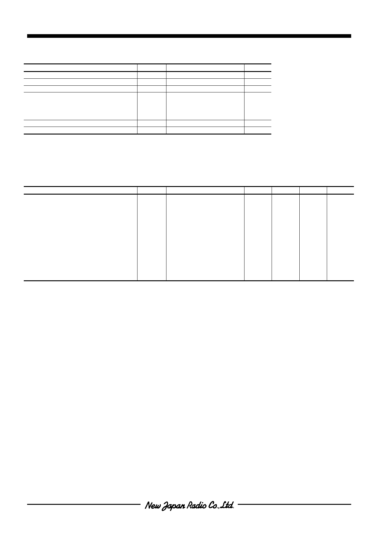
■ ABSOLUTE MAXIMUM RATINGS
PARAMETER
Supply Voltage
Differential Input Voltage
Common Mode Input Voltage
Power Dissipation
Operating Temperature Range
Storage Temperature Range
SYMBOL
VIN
VID
VIC
PD
Topr
Tstg
RATINGS
7
± 7 ( note1 )
-0.3~7
( DIP8 ) 500
( DMP8 ) 300
( SSOP8 ) 250
( TVSP8 ) 320
-40~+85
-55~+125
( Ta=25˚C )
UNIT
V
V
V
mW
˚C
˚C
( note1 ) If the supply voltage ( VDD ) is less than 7V, the input voltage must not over the VDD level though 7V is limit specified.
( note2 ) Decoupling capacitor should be connected between VDD and VSS due to the stabilized operation for the circuit.
■ ELECTRICAL CHARACTERISTICS
PARAMETER
Input Offset Voltage
Input Offset Current
Input Bias Current
Input Impedance
Large Signal Voltage Gain
Input Common Mode Voltage Range
Maximum Output Swing Voltage
Common Mode Rejection Ratio
Supply Voltage Rejection Ratio
Operating Current
Slew Rate
Unity Gain Bandwidth
SYMBOL
VIO
IIO
IIB
RIN
AVD
VICM
VOM1
VOM2
CMR
SVR
IDD
SR
Ft
TEST CONDITION
VIN=1/2VDD
RL=16kΩ
RL=16kΩ
VIN=1/2VDD
VDD=1.5~5.5V
Per Circuit
AV=40dB,CL=10pF
( note3 ) The source current is less than 181µA ( at VOM/RL=2.9V/16kΩ ).
MIN.
-
-
-
-
60
0~2.5
VDD-0.1
-
55
60
-
-
-
( Ta=25˚C,VDD=3.0V,RL=∞ )
TYP.
MAX.
UNIT
-
10
mV
1
-
pA
1
-
pA
1
-
TΩ
70
-
dB
-
-
V
-
-
V
-
VSS+0.1
V
65
-
dB
70
-
dB
0.75
1.5
mA
3.7
-
V/µs
1.0
-
MHz
-2-
Ver.2003-03-18
Share Link: 