MAX4053ACSE データシートの表示(PDF) - Maxim Integrated
部品番号
コンポーネント説明
メーカー
MAX4053ACSE Datasheet PDF : 19 Pages
| |||
Low-Voltage, CMOS Analog
Multiplexers/Switches
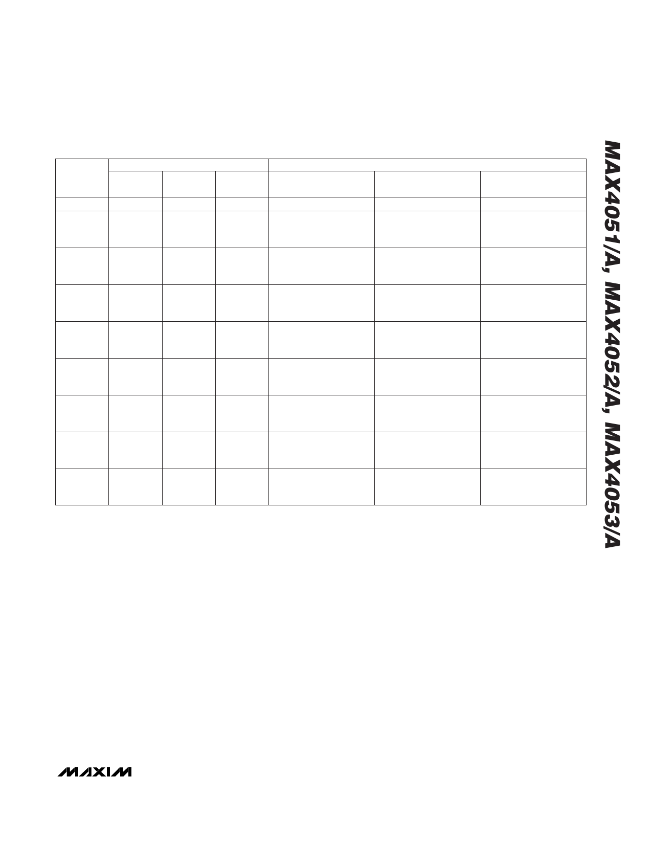
Table 1. Truth Table/Switch Programming
ADDRESS BITS
INH
ADDC*
ADDB
ADDA
MAX4051/
MAX4051A
1
X
X
X
All switches open
0
0
0
0
COM–NO0
0
0
0
1
COM–NO1
0
0
1
0
COM–NO2
0
0
1
1
COM–NO3
0
1
0
0
COM–NO4
0
1
0
1
COM–NO5
0
1
1
0
COM–NO6
0
1
1
1
COM–NO7
ON SWITCHES
MAX4052/
MAX4052A
All switches open
COMB–NO0B,
COMA–NO0A
COMB–NO1B,
COMA–NO1A
COMB–NO2B,
COMA–NO2A
COMB–NO3B,
COMA–NO3A
COMB–NO0B,
COMA–NO0A
COMB–NO1B,
COMA–NO1A
COMB–NO2B,
COMA–NO2A
COMB–NO3B,
COMA–NO3A
MAX4053/
MAX4053A
All switches open
COMA–NCA,
COMB–NCB,
COMC–NCC
COMA–NOA,
COMB–NCB,
COMC–NCC
COMA–NCA,
COMB–NOB,
COMC–NCC
COMA–NOA,
COMB–NOB,
COMC–NCC
COMA–NCA,
COMB–NCB,
COMC–NOC
COMA–NOA,
COMB–NCB,
COMC–NOC
COMA–NCA,
COMB–NOB,
COMC–NOC
COMA–NOA,
COMB–NOB,
COMC–NOC
X = Don’t care
* ADDC not present on MAX4052.
Note: NO and COM pins are identical and interchangeable. Either may be considered an input or output; signals pass equally well
in either direction.
__________Applications Information
Power-Supply Considerations
Overview
The MAX4051/MAX4052/MAX4053 and MAX4051A/
MAX4052A/MAX4053A construction is typical of most
CMOS analog switches. They have three supply pins:
V+, V-, and GND. V+ and V- are used to drive the inter-
nal CMOS switches and set the limits of the analog volt-
age on any switch. Reverse ESD-protection diodes are
internally connected between each analog signal pin
and both V+ and V-. If any analog signal exceeds V+ or
V-, one of these diodes will conduct. During normal
operation, these (and other) reverse-biased ESD diodes
leak, forming the only current drawn from V+ or V-.
Virtually all the analog leakage current comes from the
ESD diodes. Although the ESD diodes on a given signal
pin are identical, and therefore fairly well balanced,
they are reverse biased differently. Each is biased by
either V+ or V- and the analog signal. This means their
leakages will vary as the signal varies. The difference in
the two diode leakages to the V+ and V- pins consti-
tutes the analog signal path leakage current. All analog
leakage current flows between each pin and one of the
supply terminals, not to the other switch terminal. This is
why both sides of a given switch can show leakage cur-
rents of either the same or opposite polarity.
There is no connection between the analog signal
paths and GND.
______________________________________________________________________________________ 11
Share Link: 