CGY60(2000) データシートの表示(PDF) - Infineon Technologies
部品番号
コンポーネント説明
メーカー
CGY60 Datasheet PDF : 10 Pages
| |||
CGY 60
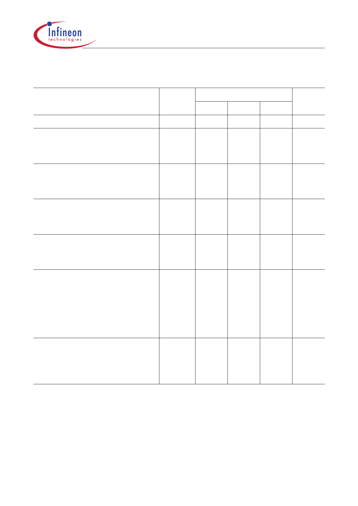
Electrical Characteristics in PCN-, DECT-Application Circuit
TA = 25 °C, f = 1850 MHz, RS = RL = 50 Ω, unless otherwise specified.
Characteristics
Symbol
Limit Values
min. typ. max.
Drain current
Power Gain
Ud = 3 V
Ud = 5 V
Noise figure
Ud = 3 V
Ud = 5 V
Input return loss
Ud = 3 V
Ud = 5 V
Output return loss
Ud = 3 V
Ud = 5 V
Third order input intercept point
two-tone intermodulation test
f1 = 1850 MHz, f2 = 1851 MHz
Pin = – 20 dBm (both carriers)
Ud = 3 V
Ud = 5 V
Input power at
1 dB gain compression
Ud = 3 V
Ud = 5 V
ID
–
G
–
–
F
–
–
RLin
–
–
RLout
–
–
IP3
–
–
P– 1 dB
–
–
6
9
12.5 –
13.5 –
1.90 –
1.85 –
14.5 –
14.5 –
14
–
14
–
0
–
2
–
–7
–
–5
–
Unit
mA
dB
dB
dB
dB
dBm
dBm
Data Book
3
03.00
Share Link: 