CGY180 データシートの表示(PDF) - Infineon Technologies
部品番号
コンポーネント説明
メーカー
CGY180 Datasheet PDF : 17 Pages
| |||
CGY 180
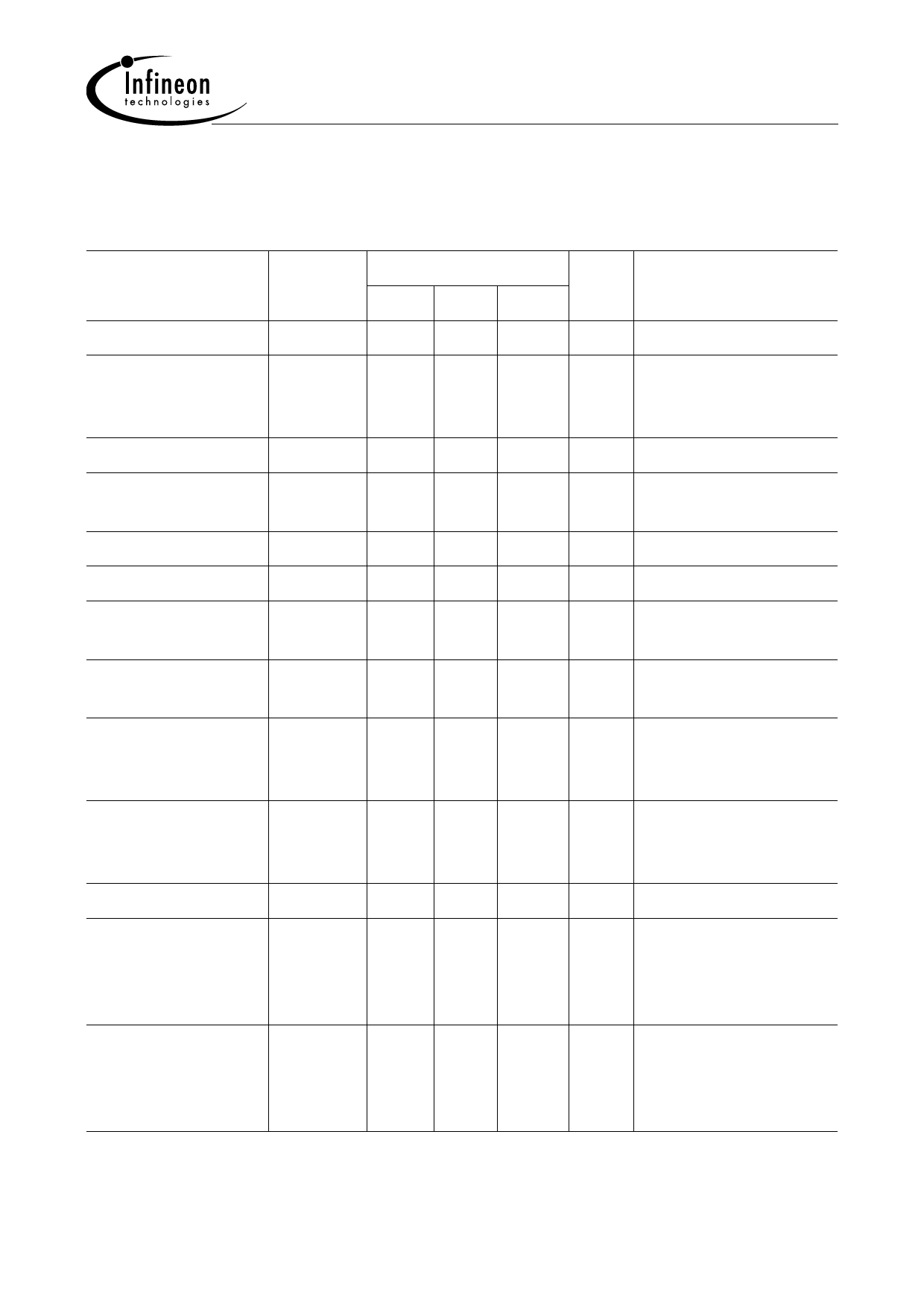
Electrical Characteristics
TA = 25 °C, f = 1.89 GHz, ZS = ZL = 50 Ω, VD = 3 V, Vg = – 4 V, VTR pin connected to
ground; unless otherwise specified
Characteristics
Symbol
Limit Values Unit Test
min. typ. max.
Conditions
Supply current
IDD
Negative supply
IG
current
(transmit operation)
–
450 –
mA Pin = 0 dBm
–
1
2.5 mA –
Shut-off current
ID
Negative supply
IG
current
–
50 180 µA VTR n.c.
–
10 50
µA shut off mode, VTR pin
n.c.
Gain
G
Output Power
Po
Output Power
Po
Overall Power
η
added Efficiency
28 30 –
25.5 27 –
–
30 –
30 35 –
dB
dBm
dBm
%
Pin = – 20 dBm
Pin = 0 dBm
VD = 5 V;
Pin = 0 dBm
Pin = 0 dBm
Harmonics 2 f0 –
3 f0 –
Harmonics 2 f0 –
3 f0 –
Input VSWR
–
Third order intercept IP3
point
Third order intercept IP3
point
–
–
– 28 dBc Pin = 0 dBm,
–
–
– 25
VD = 3 V
Pout = 27 dBm
–
–
– 25 dBc Pin = 0 dBm,
–
–
– 22
VD = 5 V,
Pout = 30 dBm
–
2:1 2.5:1 –
VD = 3 V
–
33.5 –
dBm
VD = 3 V; pulsed with a
duty cycle of 10%;
f1 = 1.8900 GHz;
f2 = 1.891728 GHz
–
38.5 –
dBm
VD = 4.8 V; pulsed with
a duty cycle of 10%;
f1 = 1.8900 GHz;
f2 = 1.891728 GHz
Data Book
4
03.00
Share Link: 