CGY180 データシートの表示(PDF) - Siemens AG
部品番号
コンポーネント説明
メーカー
CGY180 Datasheet PDF : 15 Pages
| |||
GaAs MMIC
CGY 180
_________________________________________________________________________________________________________
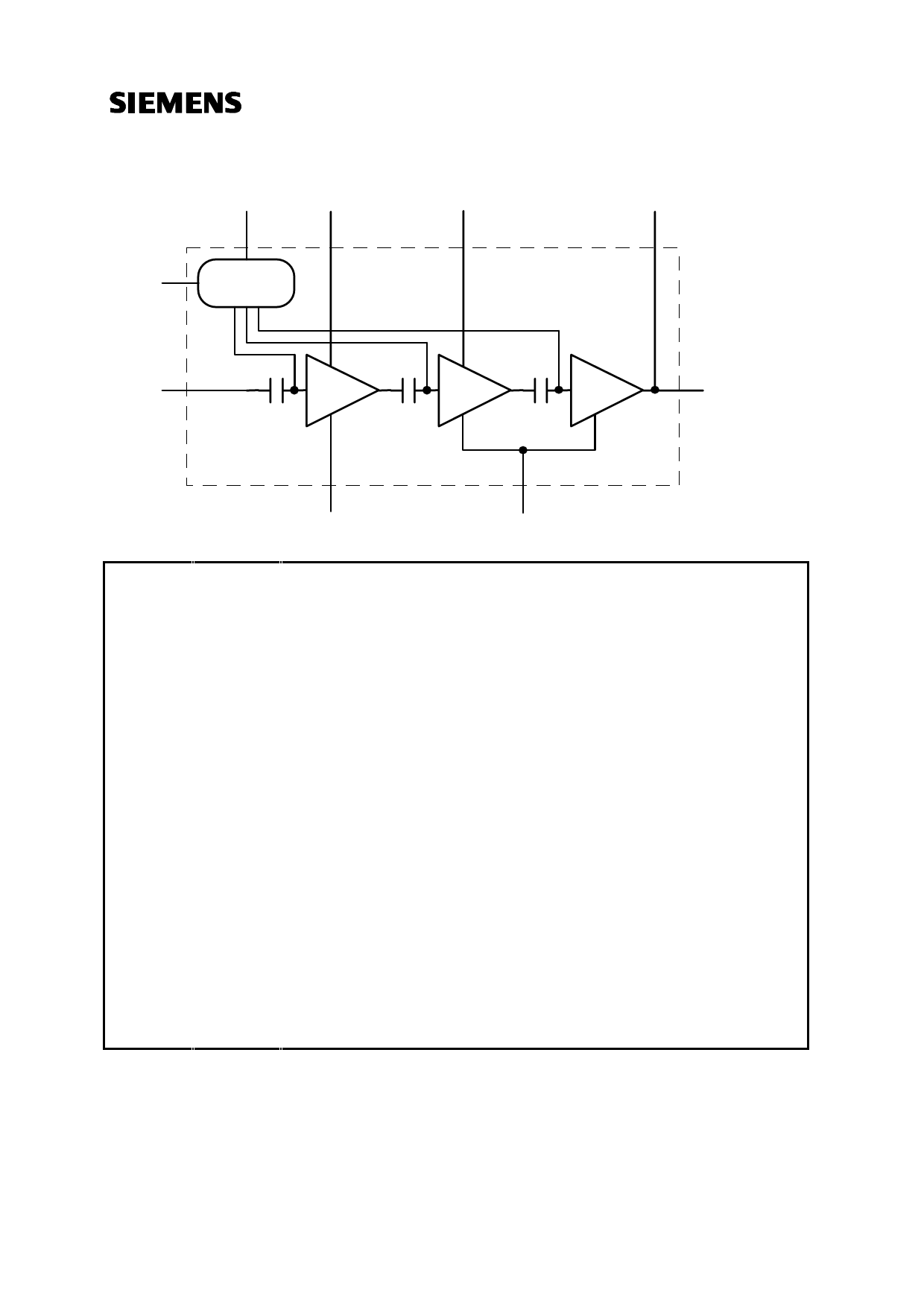
Functional Block Diagram:
VG (2)
VD1 (8)
VD2 (9)
VD3 (11)
VTR (1)
Control
circuit
Pin (7)
Pout (11)
GND1 (6)
GND2 (3,4,5,10)
Pin #
1
2
3
4
5
6
7
8
9
10
11
12
Configuration
VTR Control voltage for transmit (0V) / receive (open) mode
VG Negative voltage at control circuit (-4V...-8V)
GND2 RF and DC ground of the 2nd and 3rd stage
GND2 RF and DC ground of the 2nd and 3rd stage
GND2 RF and DC ground of the 2nd and 3rd stage
GND1 RF and DC ground of the 1st stage
RFin RF input power
VD1 Pos. drain voltage of the 1st stage
VD2 Pos. drain voltage of the 2nd stage
GND2 RF and DC ground of the 2nd and 3rd stage
VD3, Pout Pos. drain voltage of the 3rd stage, RF output power
n.c.
Siemens Aktiengesellschaft
pg. 2/15
21.02.96
HL EH PD 21
Share Link: 