CGY180 データシートの表示(PDF) - Siemens AG
部品番号
コンポーネント説明
メーカー
CGY180 Datasheet PDF : 15 Pages
| |||
GaAs MMIC
CGY 180
_________________________________________________________________________________________________________
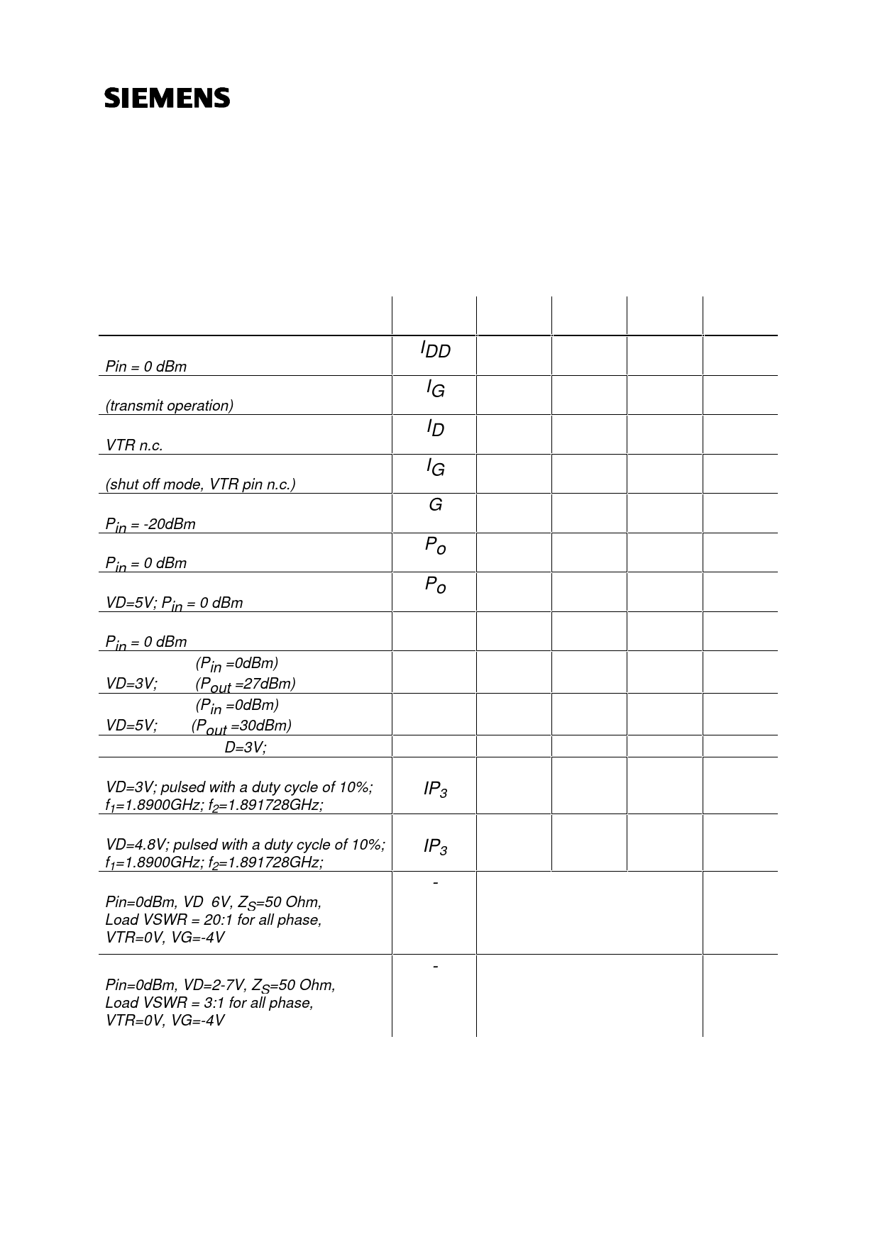
Electrical characteristics
(TA = 25°C , f=1.89 GHz, ZS=ZL=50 Ohm, VD=3.0V, VG=-4V, VTR pin connected to
ground, unless otherwise specified)
Characteristics
Symbol
Supply current
IDD
Pin = 0 dBm
Negative supply current
IG
(transmit operation)
Shut-off current
ID
VTR n.c.
Negative supply current
IG
(shut off mode, VTR pin n.c.)
Gain
G
Pin = -20dBm
Output Power
Po
Pin = 0 dBm
Output Power
Po
VD=5V; Pin = 0 dBm
Overall Power added Efficiency
η
Pin = 0 dBm
Harmonics (Pin =0dBm)
2f0
-
VD=3V;
(Pout =27dBm)
3f0
-
Harmonics (Pin =0dBm)
2f0
-
VD=5V; (Pout =30dBm)
3f0
-
Input VSWR VD=3V;
-
Third order intercept point
VD=3V; pulsed with a duty cycle of 10%;
IP3
f1=1.8900GHz; f2=1.891728GHz;
Third order intercept point
VD=4.8V; pulsed with a duty cycle of 10%;
IP3
f1=1.8900GHz; f2=1.891728GHz;
Load mismatch
-
Pin=0dBm, VD≤6V, ZS=50 Ohm,
Load VSWR = 20:1 for all phase,
VTR=0V, VG=-4V
Stability
-
Pin=0dBm, VD=2-7V, ZS=50 Ohm,
Load VSWR = 3:1 for all phase,
VTR=0V, VG=-4V
min
typ
max
-
450
-
-
1
2.5
-
50
180
-
10
50
28
30
-
25.5
27
-
-
30
-
30
35
-
-
-
-28
-
-
-25
-
-
-25
-
-
-22
-
2 : 1 2.5 : 1
-
33.5
-
-
38.5
-
No module damage
for 10 sec.
All spurious output
more than 60 dB below
desired signal level
Unit
mA
mA
µA
µA
dB
dBm
dBm
%
dBc
dBc
-
dBm
dBm
-
-
Siemens Aktiengesellschaft
pg. 4/15
21.02.96
HL EH PD 21
Share Link: 