CGY121A データシートの表示(PDF) - Siemens AG
部品番号
コンポーネント説明
メーカー
CGY121A Datasheet PDF : 8 Pages
| |||
CGY 121 A
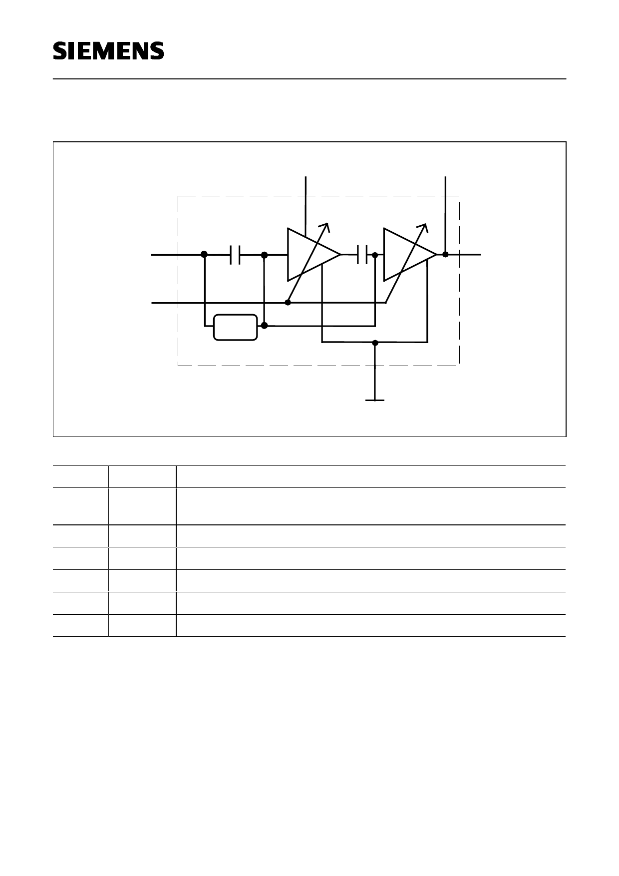
Functional block diagram:
Pin / -VG(4)
Vcon (6)
Control
Circuit
VD1 (3)
VD2 (1)
Pout (1)
GND (2, 5)
Pin #
1
2
3
4
5
6
Name Configuration
VD2 / Drain voltage 2nd stage / RF-0utput
Pout
RF-Gnd
VD1 Drain voltage 1st stage
VG / Pin Negative voltage at current control circuit (-4V) / RF-Input
RF-Gnd
Vcontrol Positive voltage for gain control (0V....3V)
Siemens Aktiengesellschaft
2
Semiconductor Group
2
23.06.98
HL HF PE GaAs1
1998-11-01
Share Link: 