CGY191 データシートの表示(PDF) - Siemens AG
部品番号
コンポーネント説明
メーカー
CGY191 Datasheet PDF : 11 Pages
| |||
CGY 191
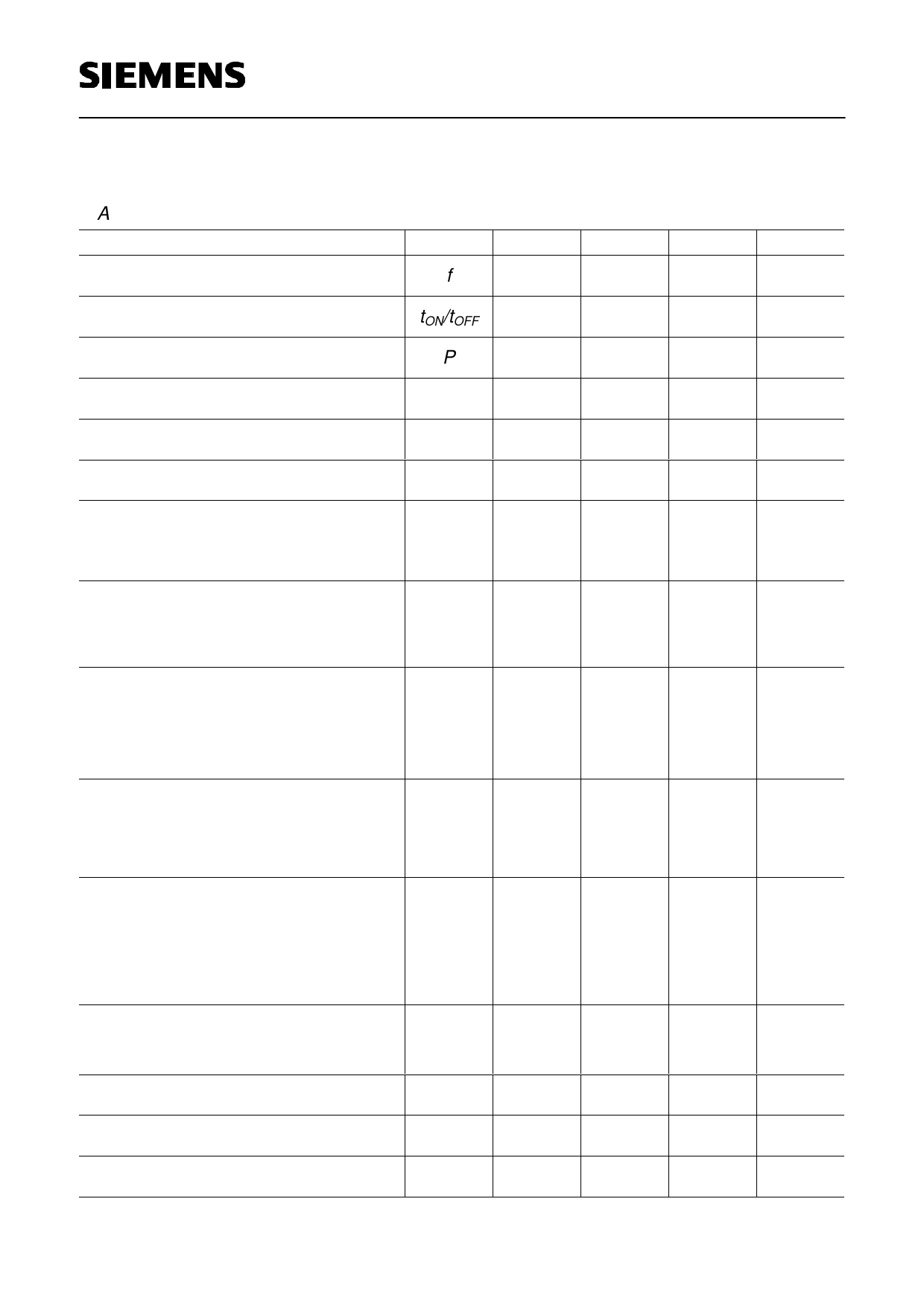
Electrical Characteristics
(TA = 25°C , ZS=ZL=50 Ohm, VD=3.5V, IDq=300mA, unless otherwise specified )
Characteristics
Symbol min
typ
max
Frequency range
f
1850
1910
Unit
MHz
Duty cycle
TDMA output power
tON/tOFF
P
100
%
29
dBm
TDMA gain at max. output
G
24
dB
CDMA output power
P
29
dBm
CDMA gain at max. output
G
24
dB
Power ramping characteristic
Full output power
Pinch off
Adjacent Channel Power CDMA
1.25 MHz offset (PCS band)
1.98 MHz offset
Adjacent channel power TDMA
adjacent
alternate
2nd alternate
Vcontr
Padj/Pmain
Padj/Pmain
V
2.5
0.5
dBc @
-45
30kHz
-54
dBc @
-28
30kHz
-45
-45
TDMA DC to RF efficiency
PAE
%
@Padj=-26dBc
at max. output
40
CDMA DC to RF efficiency
@Padj=-42dBc
at max. output
at 10 dBm output power
Receive band noise power density
( 1930 to 1990 MHz )
DC supply voltage range
Negative supply voltage range
Standby current @Vcon=0V
PAE
PRX
VD
2.9
Vneg
-5.0
Ipwr dwn
%
40
4
dBm/Hz
-145
3.5
4.0
V
-7.0
V
500
µA
Siemens Aktiengesellschaft
3
Semiconductor Group
3
23.07.1998
HL HF PE 1G9a9A8s-111/-F0o1
Share Link: 