IN74LS161D データシートの表示(PDF) - IK Semicon Co., Ltd
部品番号
コンポーネント説明
メーカー
IN74LS161D Datasheet PDF : 6 Pages
| |||
TECHNICAL DATA
Synchronous 4 Bit Counters; Binary,
Direct Reset
IN74LS161
This synchronous, presettable counter features an internal carry look-
ahead for application in high-speed counting designs. Synchronous
operation is provided by having all flip-flops clocked simultaneously so
that the outputs change conicident with each other when so instructed by
the count-enable inputs and internal gating.
This mode of operation eliminates the output counting spikes that are
normally associated with asynchronous (ripple clock) counters. A buffered
clock input triggers the four flip-flops on the rising (positive-going) edge
of the clock input wave form.
This counter is fully programmable; that is the outputs may be preset
to either level. As presetting is synchronous setting up a low level at the
load input disables the counter and causes the outputs to agree with the
setup data after the next clock pulse regardless of the levels of the enable
inputs.
The carry look-ahead circuitry provides for cascading counters for n-
bit synchronous applications without additional gating. Instrumental in
accomplishiing this function are two counter-enable inputs and a ripple
carry output. Both countenable inputs (ENABLE P and ENABLE T)
must be high to count, and ENABLE T is fed forward to enable the
ripple carry output. The ripple carry output thus enabled will produce a
high-level output pulse with a duration approximately equal to the high
level portion of the QA output. The high-level overflow ripple carry
pulse can be enable successive cascaded stages. Transitions at the
ENPor ENT are allowed regardless of the level of the clock input.
ORDERING INFORMATION
IN74LS161N Plastic
IN74LS161D SOIC
TA = 0° to 70° C for all packages
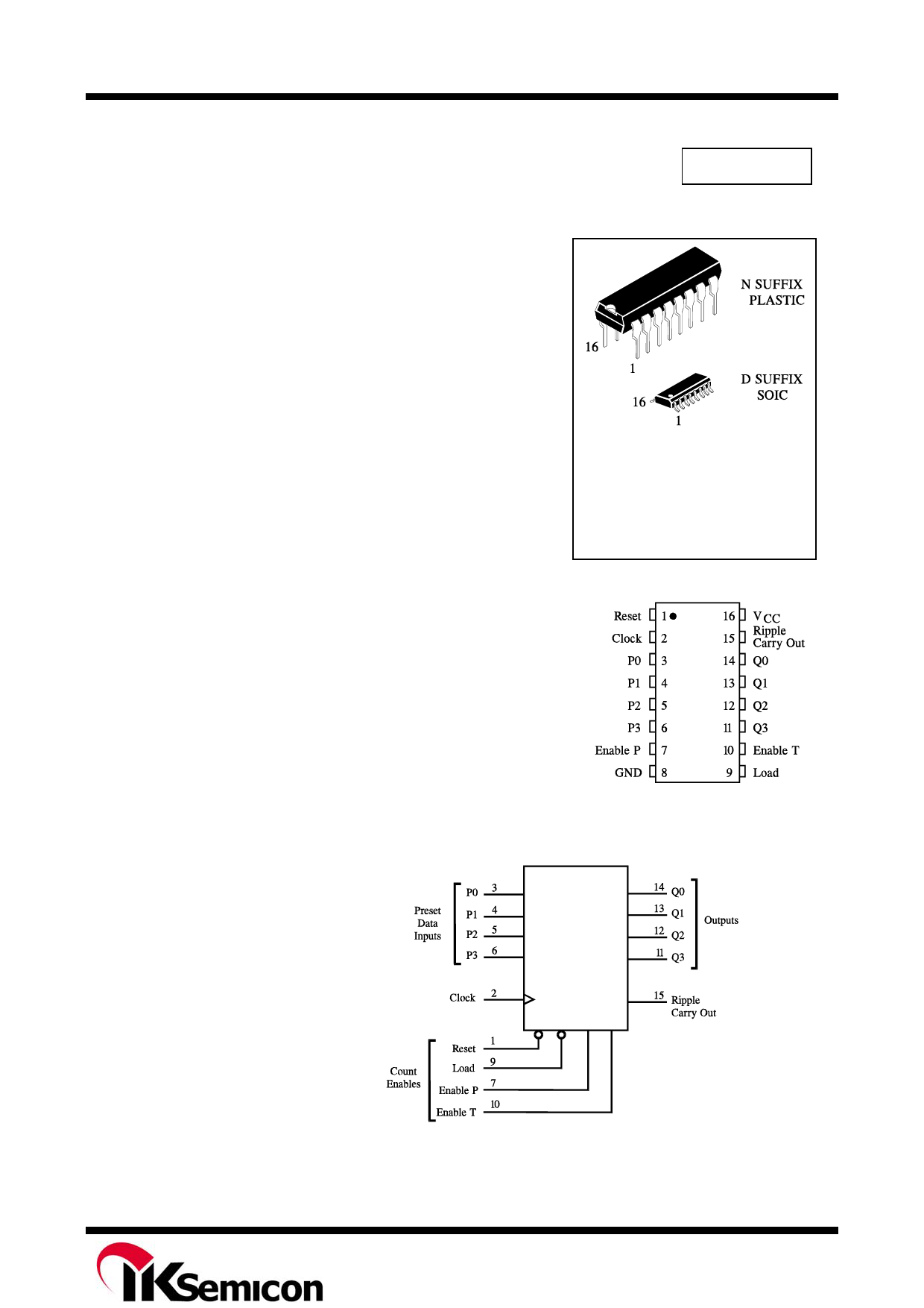
PIN ASSIGNMENT
• Internal Look-Ahead for Fast Counting
• Carry Output for n-Bit Cascading
• Synchronous Counting
• Synchronously Programmable
• Load Control Line
• Diode-Clamped Inputs
LOGIC DIAGRAM
PIN 16 =VCC
PIN 8 = GND
Rev. 00
Share Link: 