MSM9810B データシートの表示(PDF) - Oki Electric Industry
部品番号
コンポーネント説明
メーカー
MSM9810B Datasheet PDF : 45 Pages
| |||
OKI Semiconductor
FEDL9810BFULL-03
MSM9810B
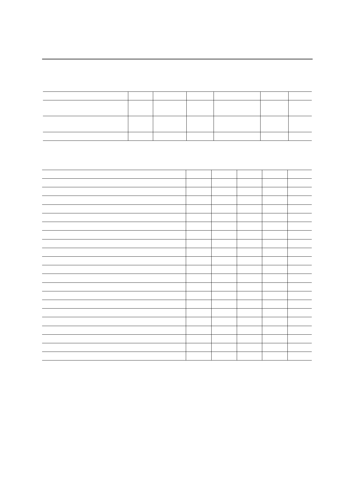
Analog Characteristics
Parameter
LDAO,RDAO Output Load
(During OP amplifier output)
LDAO,RDAO Output Impedance
(When OP amplifier is not used)
LDAO,RDAO Output Level
(DVDD = AVDD = 4.5 to 5.5 V, DGND = AGND = 0 V, Ta = –40 to +85°C)
Symbol Condition
Min.
Typ.
Max.
Unit
ROUTA
—
50
—
—
kΩ
ROUTD
—
—
3
—
kΩ
—
No load
—
0.7 to 0.94 × VDD
—
V
AC Characteristics
(VDD = 4.5 to 5.5 V, GND = 0 V, Ta = –40 to +85°C, CL = 5 pF)
Parameter
Symbol Min.
Typ.
Max.
Unit
Master Clock Duty Cycle
RESET Input Pulse Width
RESET Input Time From Raising of Power Supply
Set up and Hold Time of CS for RD
RD Pulse Width
Output Data Valid Time after Fall of RD
Data Float Time after Rise of RD
Setup and Hold Time of CMD for WR
Setup and Hold Time of CS for WR
WR Pulse Width
Data Setup Time before Rise of WR
Data Hold Time after Rise of WR
WR - WR Pulse Interval
CS - CS Pulse Interval
fduty
40
50
60
%
tW(RST)
1
—
—
µs
tD(RST)
0
—
—
µs
tCR
30
—
—
ns
tRR
200
—
—
ns
tDRE
—
—
100
ns
tDRF
—
10
50
ns
tDW
50
—
—
ns
tCW
30
—
—
ns
tWW
200
—
—
ns
tDWS
100
—
—
ns
tDWH
30
—
—
ns
tWWS
160
—
—
ns
tCC
100
—
—
ns
Serial Data Setup Time
tSDS
30
—
—
ns
Serial Data Hold Time
tSSD
30
—
—
ns
Serial Clock Pulse Width
tW(SCK)
200
—
—
ns
Output Data Valid Time after Rise of Serial Clock
Setup Time of WR for Serial Data
Setup Time of Serial Clock Fall for WR Rise
Setup Time of RD for Serial Clock Rise
tSDD
—
—
200
ns
tSWDS
200
—
—
ns
tSIWS
300
—
—
ns
tSRIS
300
—
—
ns
7/45
Share Link: 